JAJSAQ9F November 2008 – September 2016 LM27341 , LM27341-Q1 , LM27342 , LM27342-Q1
PRODUCTION DATA.
- 1 特長
- 2 アプリケーション
- 3 概要
- 4 改訂履歴
- 5 Pin Configuration and Functions
- 6 Specifications
- 7 Detailed Description
-
8 Application and Implementation
- 8.1
Application Information
- 8.1.1 Inductor Selection
- 8.1.2 Inductor Material Selection
- 8.1.3 Input Capacitor
- 8.1.4 Output Capacitor
- 8.1.5 Catch Diode
- 8.1.6 Boost Diode (Optional)
- 8.1.7 Boost Capacitor
- 8.1.8 Output Voltage
- 8.1.9 Feedforward Capacitor (Optional)
- 8.1.10
Calculating Efficiency and Junction Temperature
- 8.1.10.1 Schottky Diode Conduction Losses
- 8.1.10.2 Inductor Conduction Losses
- 8.1.10.3 MOSFET Conduction Losses
- 8.1.10.4 MOSFET Switching Losses
- 8.1.10.5 IC Quiescent Losses
- 8.1.10.6 MOSFET Driver Losses
- 8.1.10.7 Total Power Losses
- 8.1.10.8 Efficiency Calculation Example
- 8.1.10.9 Calculating Junction Temperature
- 8.2
Typical Applications
- 8.2.1 LM2734x Configuration From VIN = 7 V to 16 V, VOUT = 5 V For Full Load at 2 MHz
- 8.2.2 LM2734x Configuration From VIN = 7 V to 16 V, VOUT = 5 V For Full Load at 1 MHz
- 8.2.3 LM2734x Configuration From VIN = 5 V to 16 V, VOUT = 3.3 V For Full Load at 2 MHz
- 8.2.4 LM2734x Configuration From VIN = 5 V to 16 V, VOUT = 3.3 V For Full Load at 2 MHz With SYNC = GND
- 8.2.5 LM2734x Configuration From VIN = 5 V to 16 V, VOUT = 3.3 V For Full Load at 2 MHz With SYNC = 1 MHz
- 8.2.6 LM2734x Configuration From VIN = 3.3 V to 16 V, VOUT = 1.8 V For Full Load at 2 MHz With SYNC = 1 GND
- 8.2.7 LM2734x Configuration From VIN = 3.3 V to 16 V, VOUT = 1.8 V For Full Load at 2 MHz With SYNC = 1 MHz
- 8.2.8 LM2734x Configuration From VIN = 3.3 V to 9 V, VOUT = 1.2 V For Full Load at 2 MHz With SYNC = 2 MHz
- 8.1
Application Information
- 9 Power Supply Recommendations
- 10Layout
- 11デバイスおよびドキュメントのサポート
- 12メカニカル、パッケージ、および注文情報
パッケージ・オプション
メカニカル・データ(パッケージ|ピン)
- DGQ|10
サーマルパッド・メカニカル・データ
- DGQ|10
発注情報
6 Specifications
6.1 Absolute Maximum Ratings
over operating free-air temperature range (unless otherwise noted)(1)(2)| MIN | MAX | UNIT | ||
|---|---|---|---|---|
| AVIN, PVIN | –0.5 | 24 | V | |
| SW voltage | –0.5 | 24 | V | |
| Boost voltage | –0.5 | 28 | V | |
| Boost to SW voltage | –0.5 | 6 | V | |
| FB voltage | –0.5 | 3 | V | |
| SYNC voltage | –0.5 | 6 | V | |
| EN voltage | –0.5 | VIN + 0.3 | V | |
| Soldering, infrared reflow (5 s) | 260 | °C | ||
| Junction temperature, TJ | 150 | °C | ||
| Storage temperature, Tstg | –65 | 150 | °C | |
(1) Stresses beyond those listed under Absolute Maximum Ratings may cause permanent damage to the device. These are stress ratings only, which do not imply functional operation of the device at these or any other conditions beyond those indicated under Recommended Operating Conditions. Exposure to absolute-maximum-rated conditions for extended periods may affect device reliability.
(2) If Military/Aerospace specified devices are required, please contact the Texas Instruments Sales Office/ Distributors for availability and specifications.
6.2 ESD Ratings
| VALUE | UNIT | |||
|---|---|---|---|---|
| V(ESD) | Electrostatic discharge | Human-body model (HBM), per ANSI/ESDA/JEDEC JS-001(1)(2) | ±2000 | V |
(1) JEDEC document JEP155 states that 500-V HBM allows safe manufacturing with a standard ESD control process.
(2) Human body model, 1.5 kΩ in series with 100 pF.
6.3 Recommended Operating Conditions
over operating free-air temperature range (unless otherwise noted)(1)| MIN | MAX | UNIT | |
|---|---|---|---|
| AVIN, PVIN | 3 | 20 | V |
| SW voltage | –0.5 | 20 | V |
| Boost voltage | –0.5 | 24 | V |
| Boost to SW voltage | 3 | 5.5 | V |
| Junction temperature | –40 | 125 | °C |
(1) Absolute Maximum Ratings indicate limits beyond which damage to the device may occur, including inoperability and degradation of device reliability and/or performance. Functional operation of the device and/or non-degradation at the Absolute Maximum Ratings or other conditions beyond those indicated in the recommended Operating Ratings is not implied. The recommended Operating Ratings indicate conditions at which the device is functional and should not be operated beyond such conditions.
6.4 Thermal Information
| THERMAL METRIC(1) | LM2734x, LM2734x-Q1 | UNIT | ||
|---|---|---|---|---|
| DSC (WSON) | DGQ (MSOP-PowerPAD) | |||
| 10 PINS | 10 PINS | |||
| RθJA | Junction-to-ambient thermal resistance(2) | 47.6 | 49.5 | °C/W |
| RθJC(top) | Junction-to-case (top) thermal resistance | 36.5 | 53.6 | °C/W |
| RθJB | Junction-to-board thermal resistance | 22.5 | 33.7 | °C/W |
| ψJT | Junction-to-top characterization parameter | 0.4 | 3.9 | °C/W |
| ψJB | Junction-to-board characterization parameter | 22.7 | 33.4 | °C/W |
| RθJC(bot) | Junction-to-case (bottom) thermal resistance | 4.7 | 3.5 | °C/W |
(1) For more information about traditional and new thermal metrics, see the Semiconductor and IC Package Thermal Metrics application report.
(2) Thermal shutdown will occur if the junction temperature exceeds 165°C. The maximum power dissipation is a function of TJ(MAX), RθJA and TA. The maximum allowable power dissipation at any ambient temperature is PD = (TJ(MAX) – TA)/ RθJA. All numbers apply for packages soldered directly onto a 3" × 3" PCB with 2 oz. copper on 4 layers in still air.
6.5 Electrical Characteristics
TJ = 25°C, VIN = 12 V, and VBOOST – VSW = 4.3 V (unless otherwise noted)| PARAMETER | TEST CONDITIONS | MIN | TYP | MAX | UNIT | ||
|---|---|---|---|---|---|---|---|
| SYSTEM PARAMETERS | |||||||
| VFB | Feedback voltage | TJ = 0°C to 85°C | 0.99 | 1 | 1.01 | V | |
| TJ = –40°C to 125°C | 0.984 | 1 | 1.014 | ||||
| ΔVFB/ΔVIN | Feedback voltage line regulation | VIN = 3 V to 20 V | 0.003% | V | |||
| IFB | Feedback input bias current | TJ = 25°C | 20 | nA | |||
| TJ = –40°C to 125°C | 100 | ||||||
| OVP | Overvoltage protection | VFB at which PWM halts | 1.13 | V | |||
| UVLO | Undervoltage lockout | VIN rising until VSW is switching | TJ = 25°C | 2.75 | V | ||
| TJ = –40°C to 125°C | 2.6 | 2.9 | |||||
| Undervoltage hysteresis | VIN falling from UVLO | TJ = 25°C | 0.47 | ||||
| TJ = –40°C to 125°C | 0.3 | 0.6 | |||||
| SS | Soft-start time | 0.5 | 1 | 1.5 | ms | ||
| IQ | Quiescent current | IQ = IQ_AVIN + IQ_PVIN | VFB = 1.1 (not switching) | 2.4 | mA | ||
| VEN = 0 V (shutdown) | 70 | nA | |||||
| IBOOST | Boost pin current | fSW= 2 MHz | TJ = 25°C | 8.2 | mA | ||
| TJ = –40°C to 125°C | 10 | ||||||
| fSW= 1 MHz | 4.4 | 6 | |||||
| OSCILLATOR | |||||||
| fSW | Switching frequency | SYNC = GND | TJ = 25°C | 2 | MHz | ||
| TJ = –40°C to 125°C | 1.75 | 2.3 | |||||
| VFB_FOLD | FB pin voltage | SYNC input is overridden | 0.53 | V | |||
| fFOLD_MIN | Frequency foldback minimum | VFB = 0 V | 220 | 250 | kHz | ||
| LOGIC INPUTS (EN, SYNC) | |||||||
| fSYNC | SYNC frequency range | 1 | 2.35 | MHz | |||
| VIL | EN, SYNC logic low threshold | Logic falling edge | 0.4 | V | |||
| VIH | EN, SYNC logic high threshold | Logic rising edge | 1.8 | ||||
| tSYNC_HIGH | SYNC, time required above VIH to ensure a logical high | 100 | ns | ||||
| tSYNC_LOW | SYNC, time required below VIL to ensure a logical low | 100 | ns | ||||
| ISYNC | SYNC pin current | VSYNC < 5 V | 20 | nA | |||
| IEN | Enable pin current | VEN = 3 V | 6 | 15 | µA | ||
| VIN = VEN = 20 V | 50 | 100 | |||||
| INTERNAL MOSFET | |||||||
| RDS(ON) | Switch ON-resistance | TJ = 25°C | 150 | mΩ | |||
| TJ = –40°C to 125°C | 320 | ||||||
| ICL | Switch current limit | TJ = –40°C to 125°C | LM27342 | 2.5 | 4 | A | |
| LM27341 | 2 | 3.7 | |||||
| DMAX | Maximum duty cycle | SYNC = GND | TJ = 25°C | 93% | |||
| TJ = –40°C to 125°C | 85% | ||||||
| tMIN | Minimum ON-time | 65 | ns | ||||
| ISW | Switch leakage current | 40 | nA | ||||
| BOOST LDO | |||||||
| VLDO | Boost LDO output voltage | 3.9 | V | ||||
| THERMAL | |||||||
| TSHDN | Thermal shutdown temperature | Junction temperature rising | 165 | °C | |||
| Thermal shutdown hysteresis | Junction temperature falling | 15 | |||||
6.6 Typical Characteristics
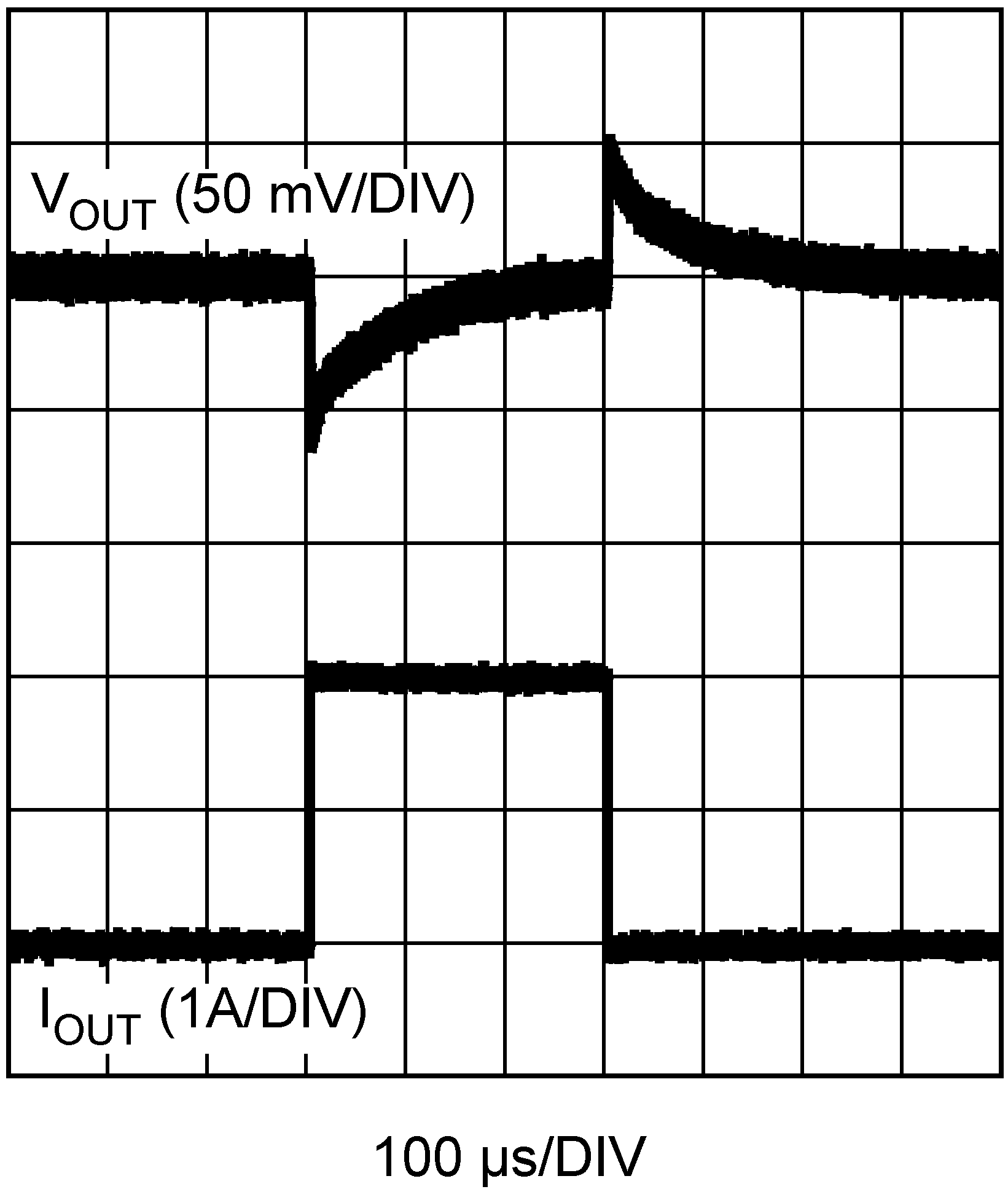
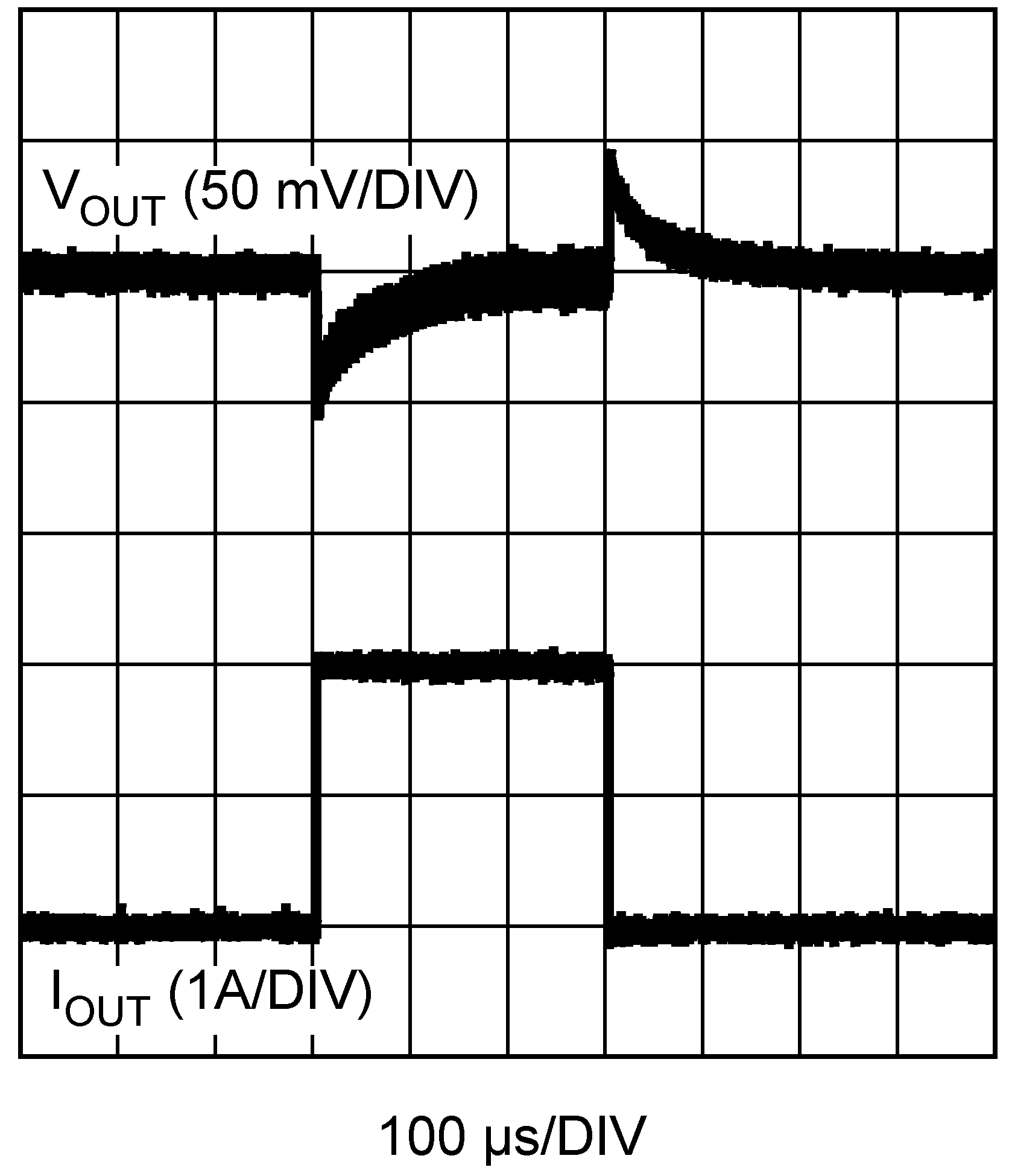
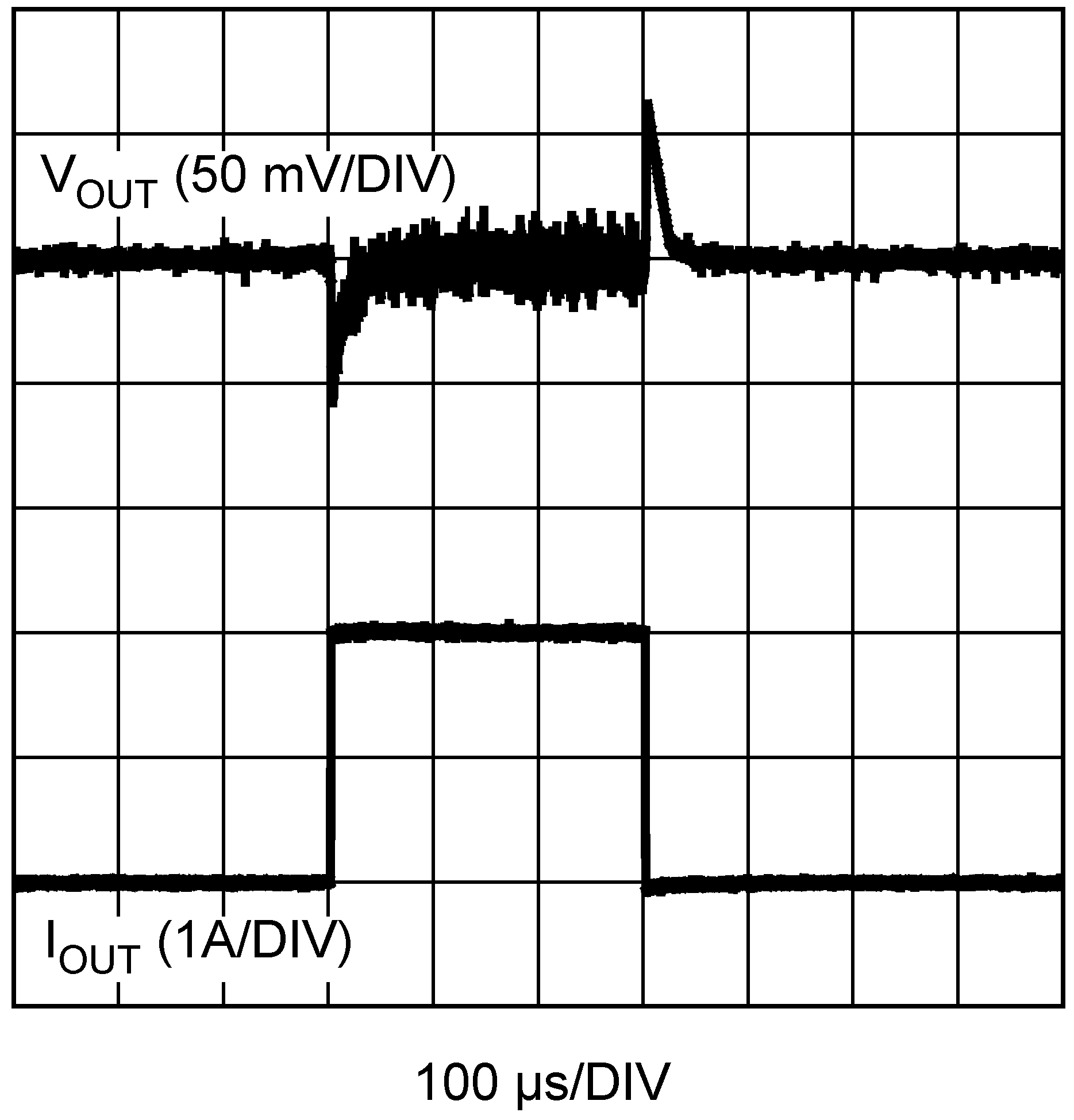
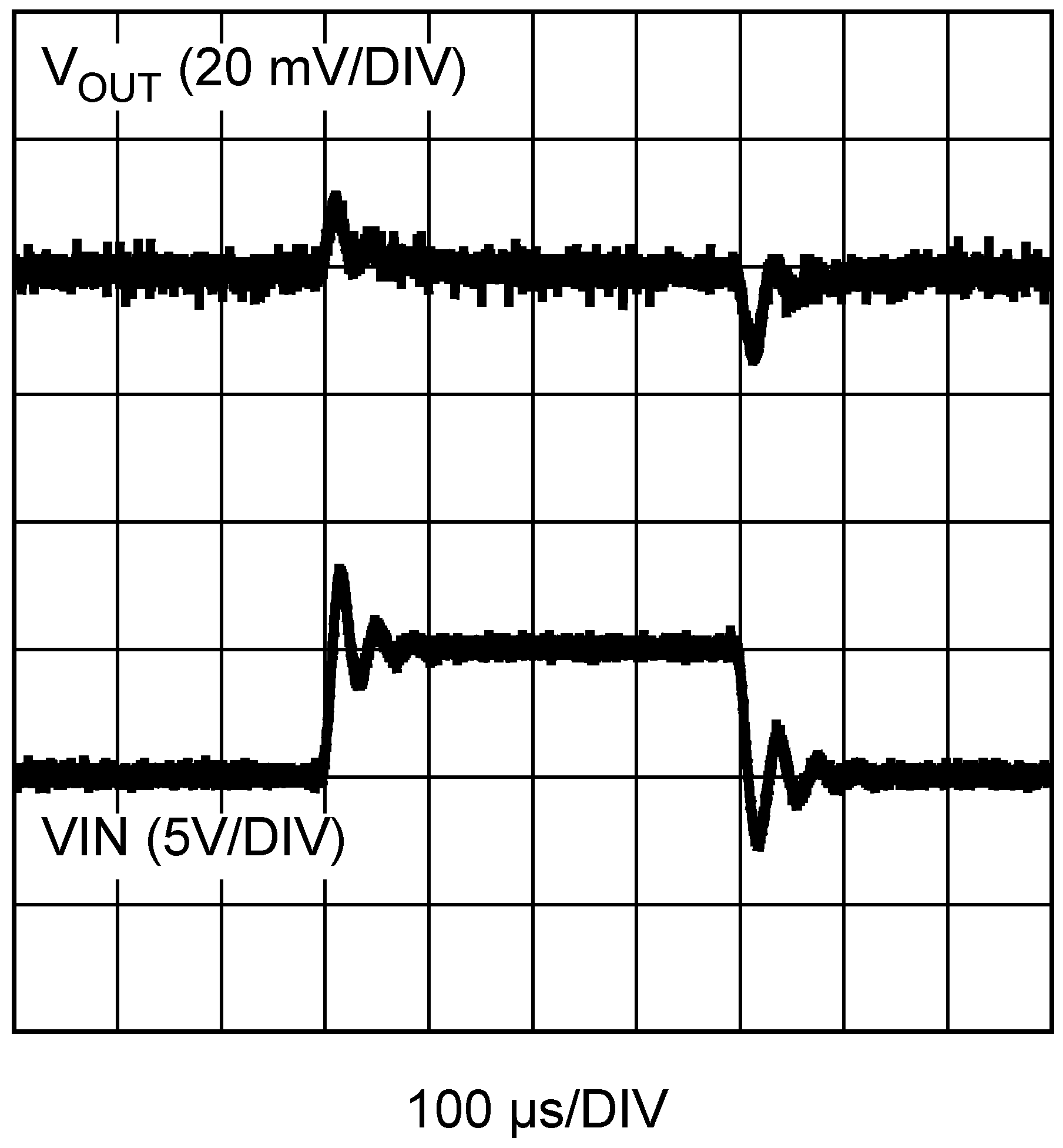
TA = 25°C, VIN = 12 V, and VBOOST – VSW = 4.3 V (unless otherwise noted)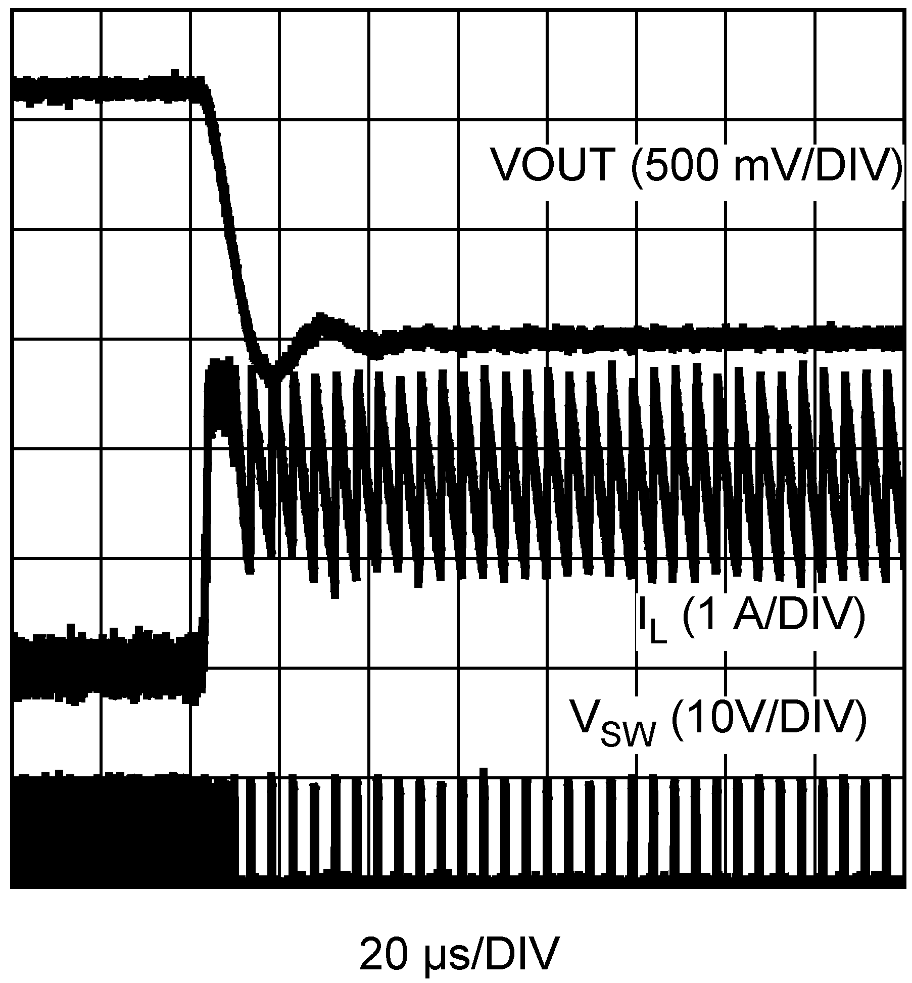 Figure 9. Short Circuit
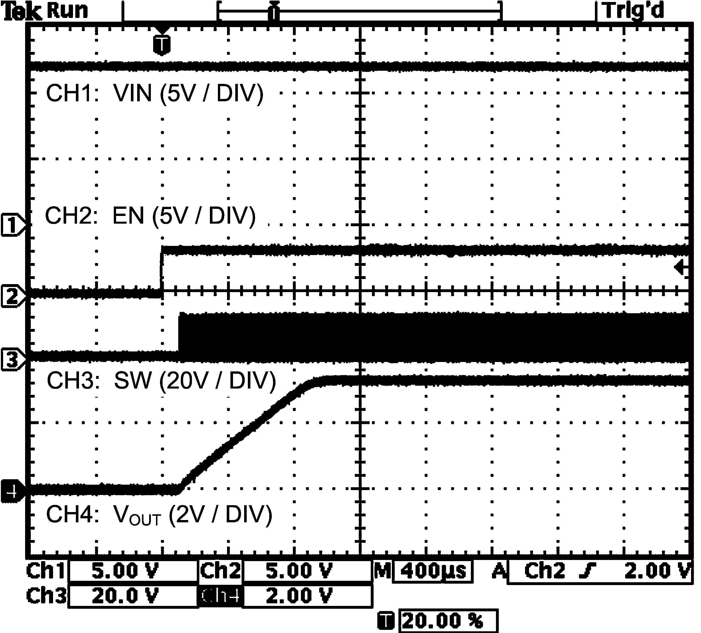 Figure 11. Soft Start With EN Tied to VIN
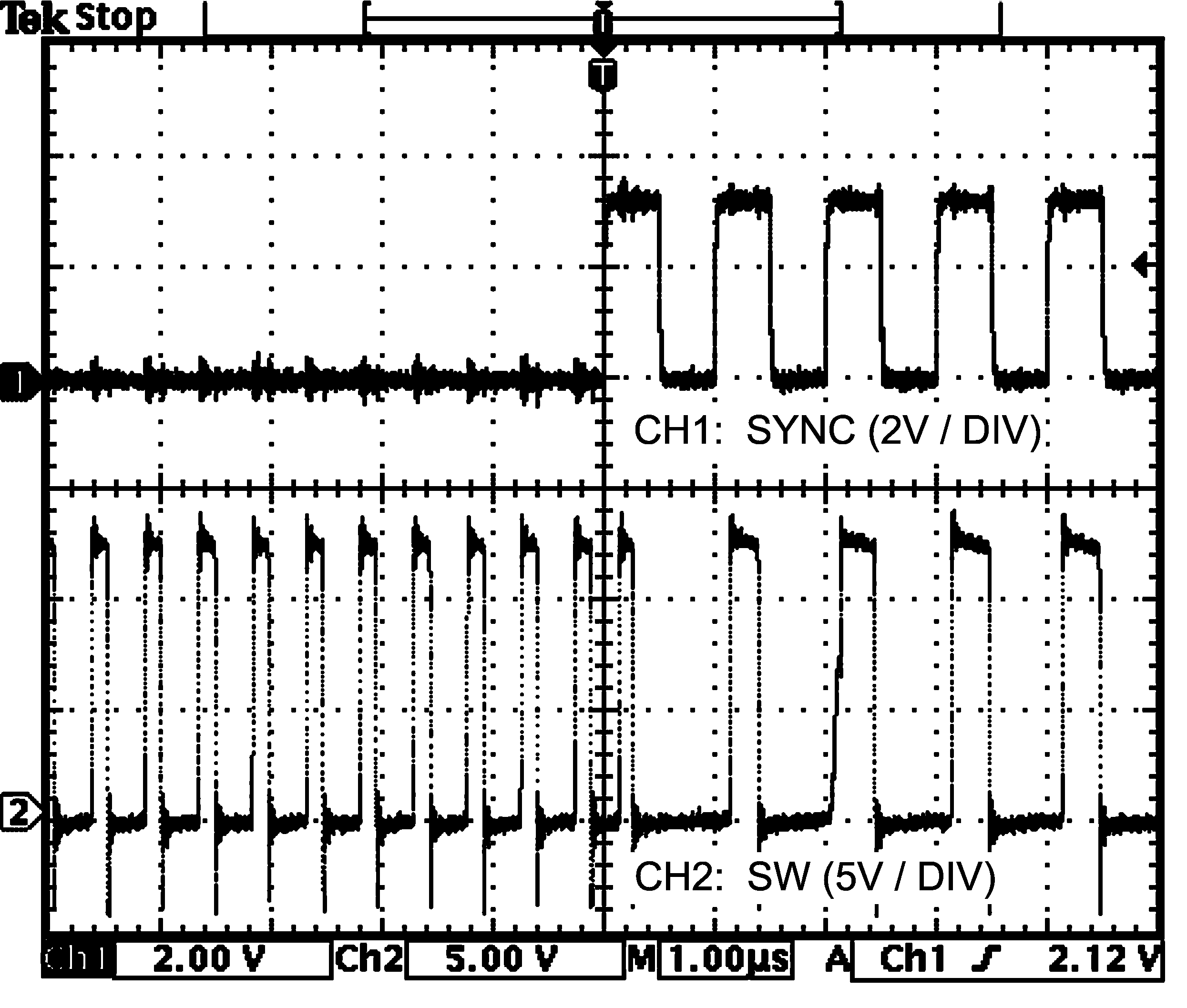 Figure 17. Sync Functionality
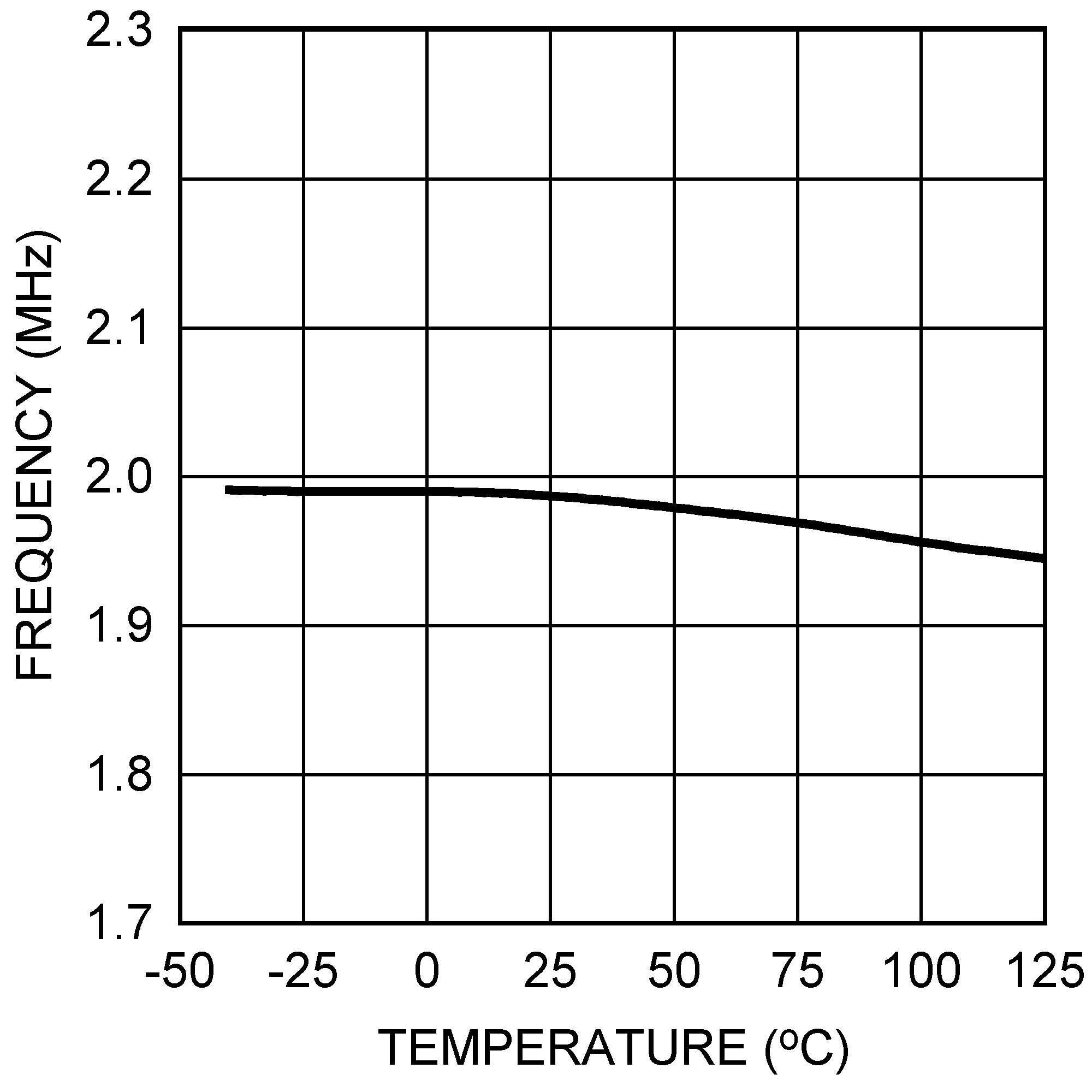
| VSYNC = GND | fSW = 2 MHz |
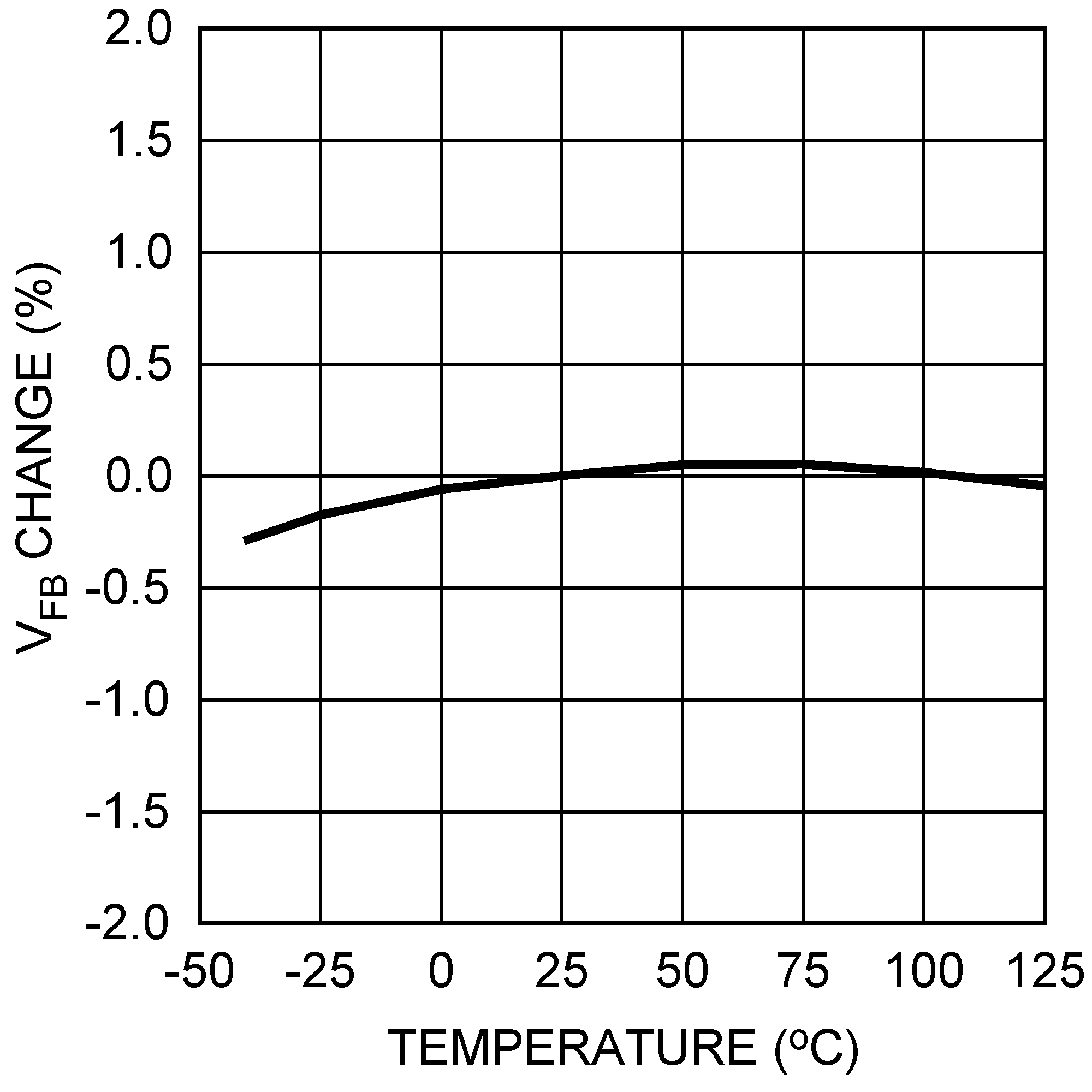 Figure 21. VFB vs Temperature
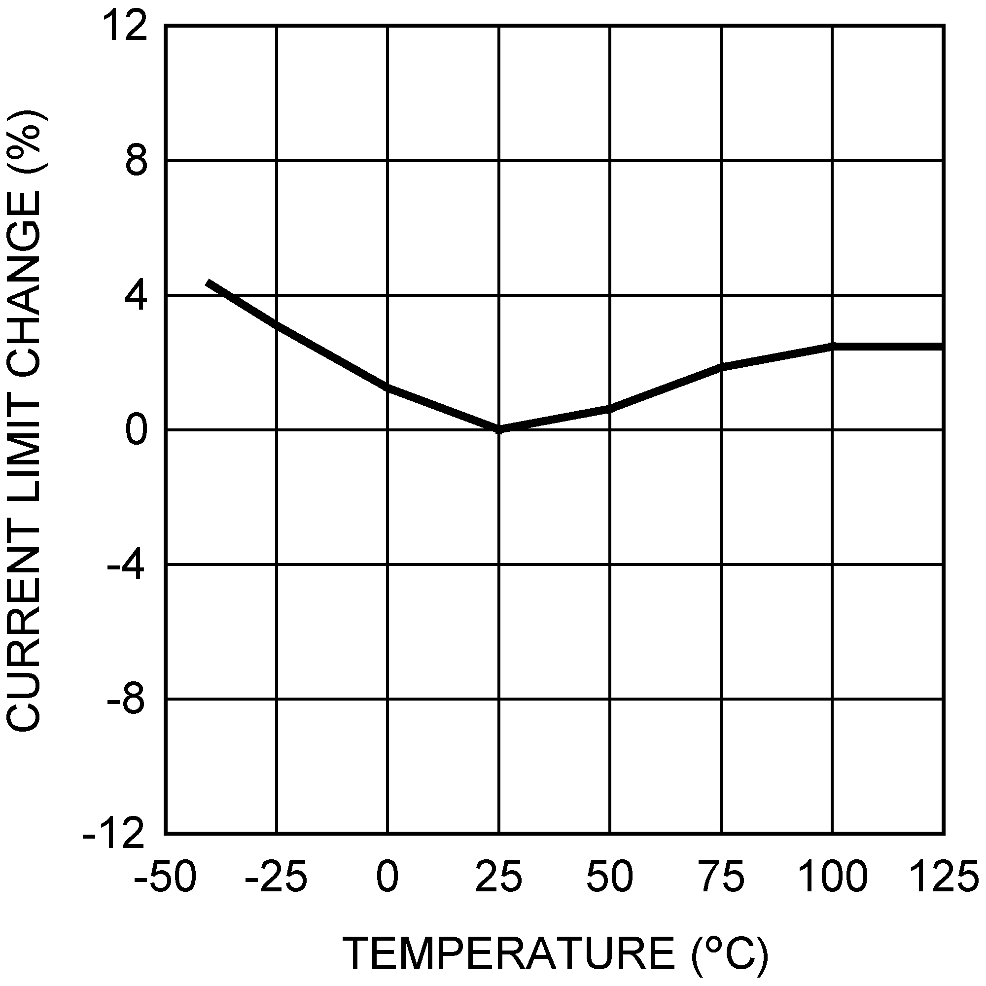
| VIN = 12 V |
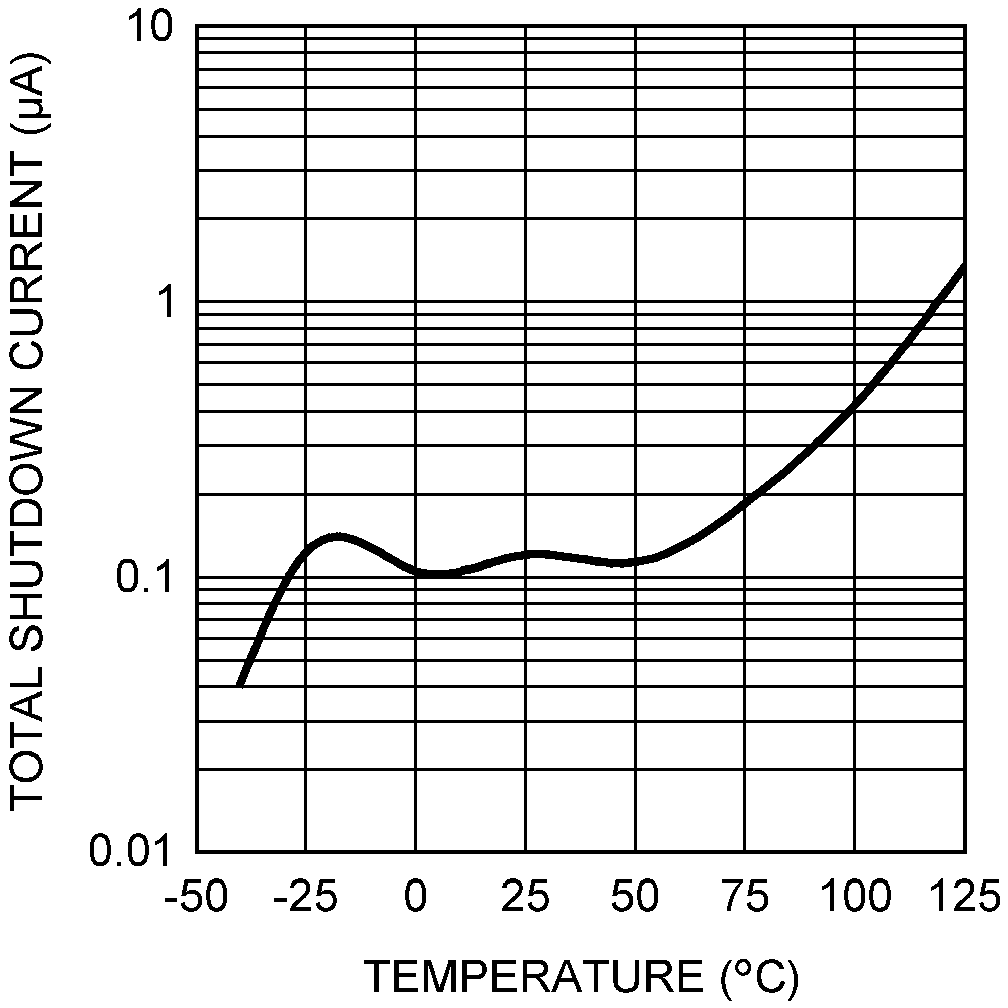
| IQ = IAVIN + IPVIN |
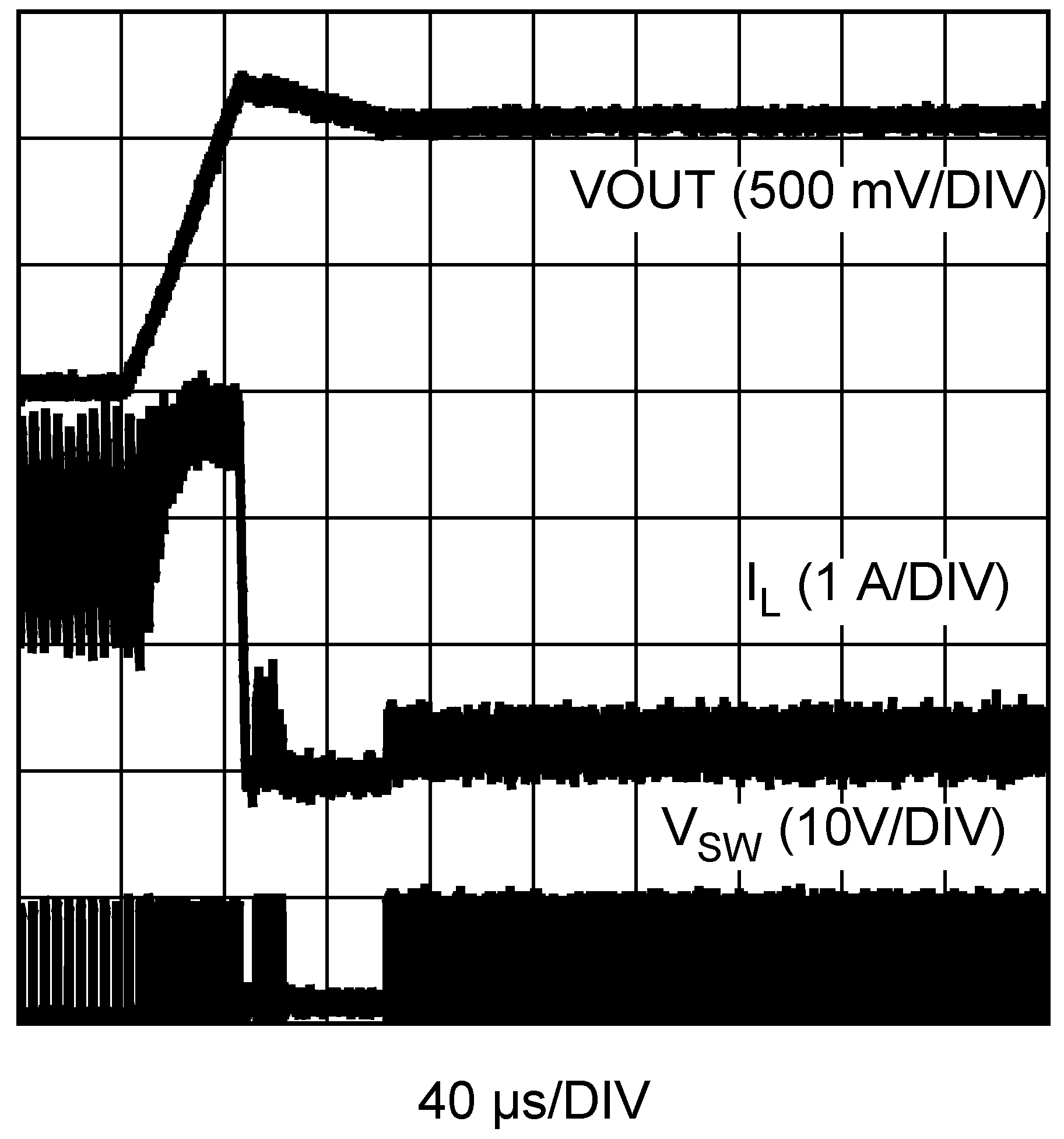 Figure 10. Short-Circuit Release
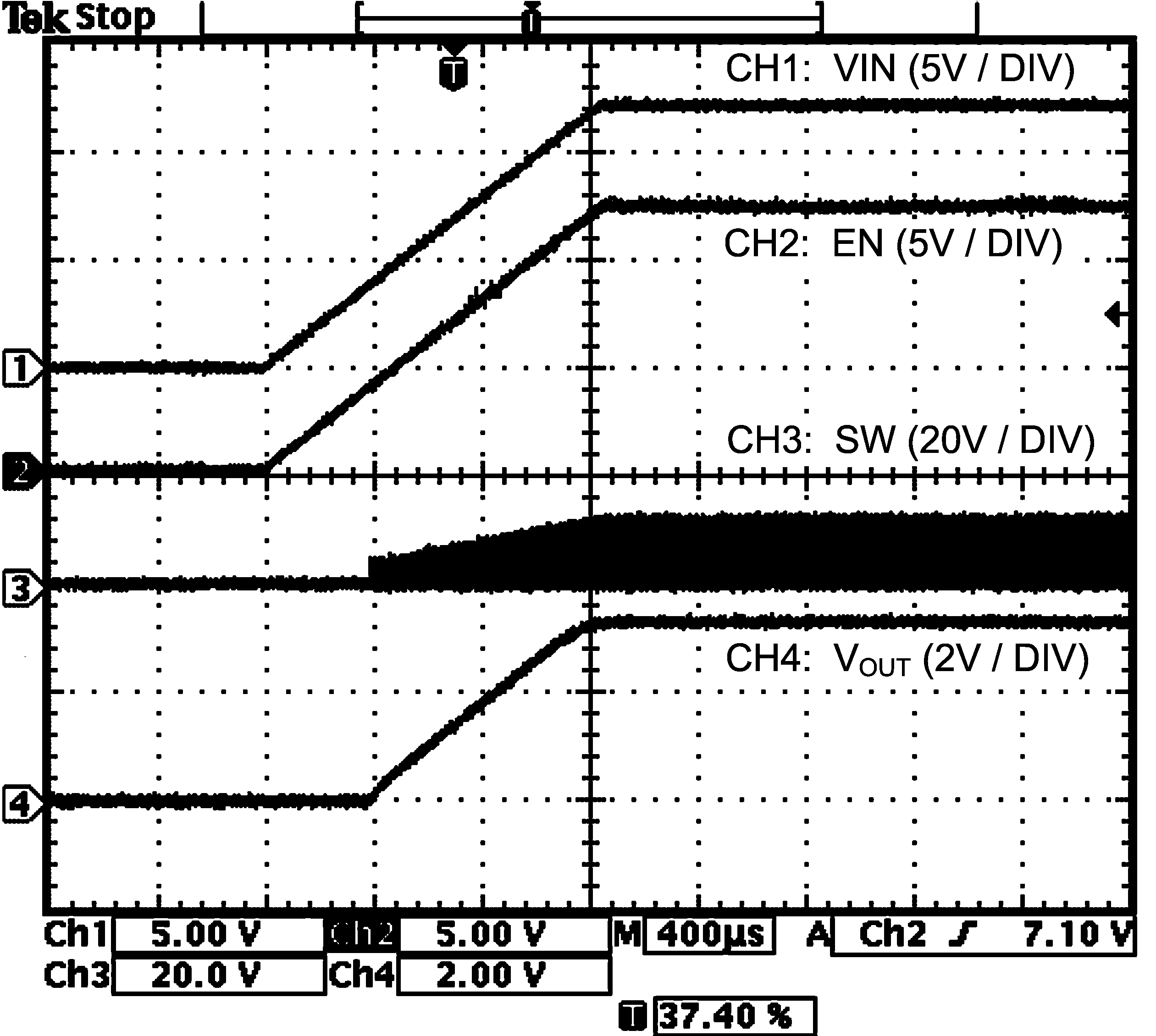 Figure 12. Soft Start With EN Tied to VIN
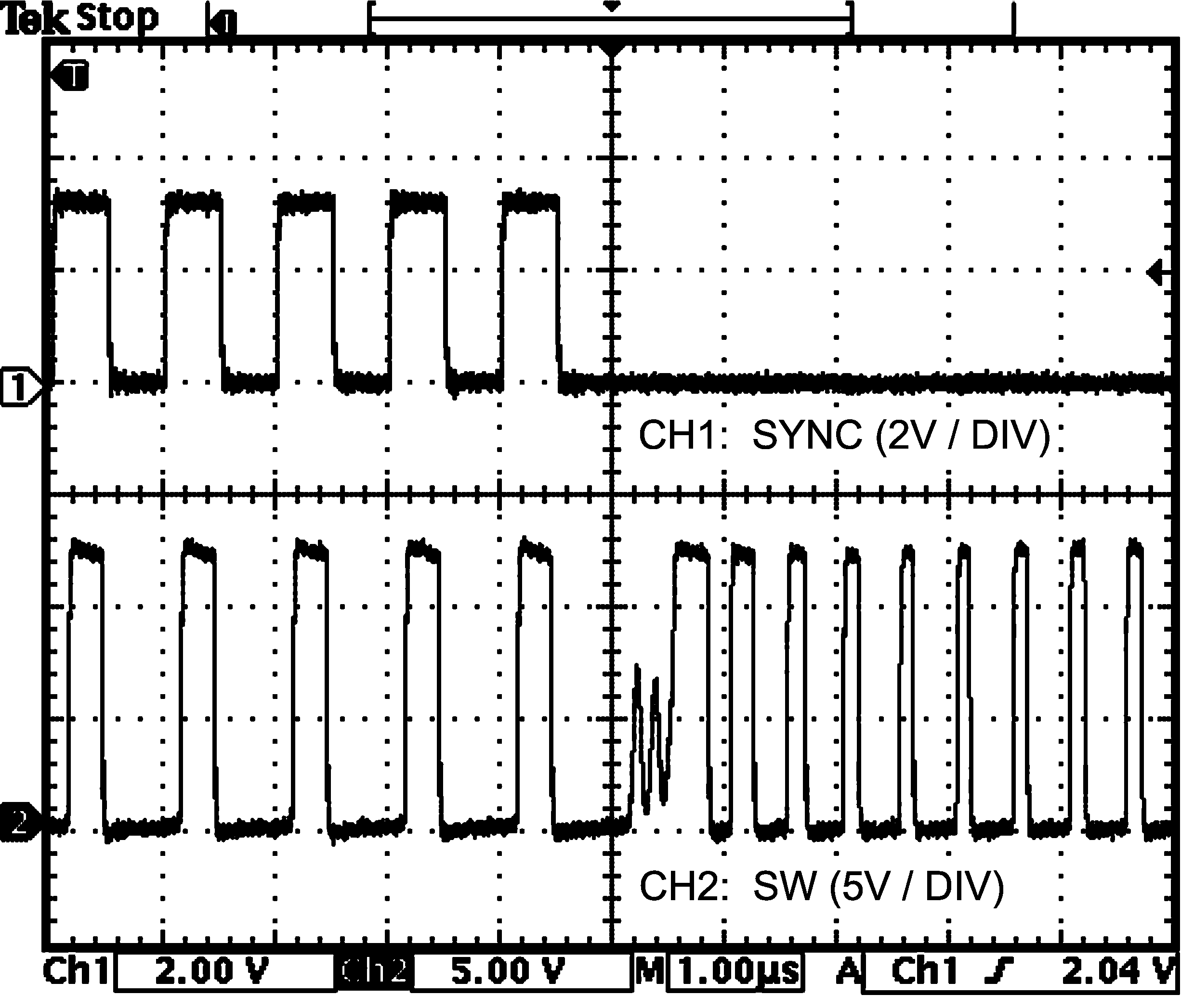 Figure 18. Loss of Synchronization
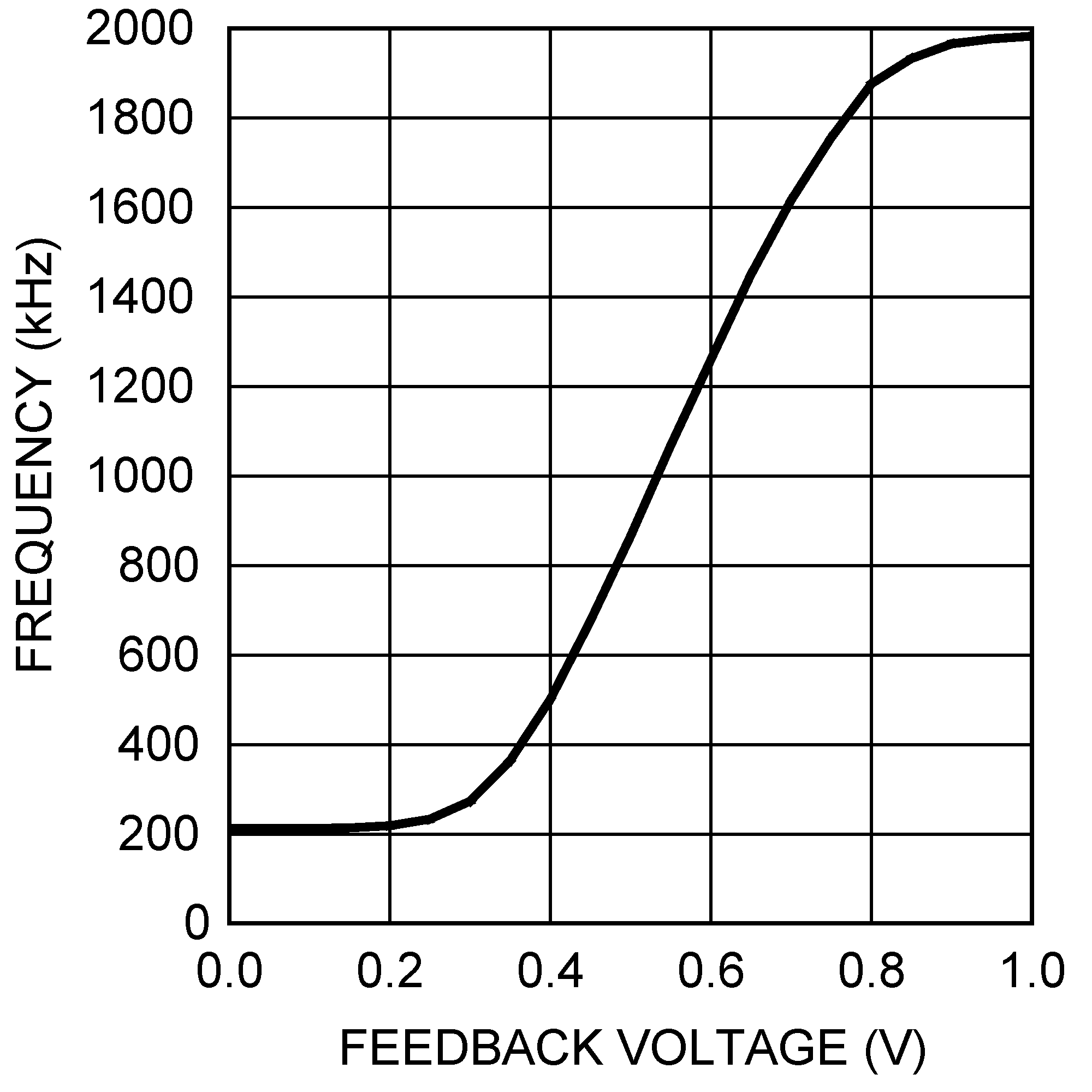
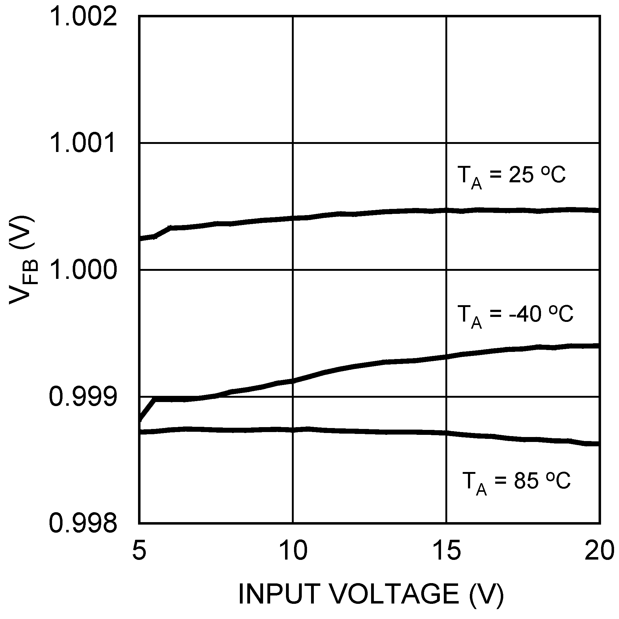 Figure 22. VFB vs VIN
