JAJSAM0A October 2006 – September 2017 LM2853
PRODUCTION DATA.
- 1 特長
- 2 アプリケーション
- 3 概要
- 4 改訂履歴
- 5 Pin Configuration and Functions
- 6 Specifications
- 7 Detailed Description
-
8 Application and Implementation
- 8.1
Application Information
- 8.1.1 Input Capacitor (CIN)
- 8.1.2 Soft-Start Capacitor (CSS)
- 8.1.3 Soft-Start Capacitor (CSS) and Fault Conditions
- 8.1.4 Compensation
- 8.1.5 Output Filter Values
- 8.1.6 Choosing an Inductance Value
- 8.1.7 Output Filter Inductors
- 8.1.8 Output Filter Capacitors
- 8.1.9 Split-Rail Operation
- 8.1.10 Switch Node Protection
- 8.2 Typical Application
- 8.1
Application Information
- 9 Layout
- 10デバイスおよびドキュメントのサポート
- 11メカニカル、パッケージ、および注文情報
パッケージ・オプション
メカニカル・データ(パッケージ|ピン)
- PWP|14
サーマルパッド・メカニカル・データ
- PWP|14
発注情報
9 Layout
9.1 Layout Guidelines
These are several guidelines to follow while designing the PCB layout for an LM2853 application.
- The input bulk capacitor, CIN, should be placed very close to the PVIN pin to keep the resistance as low as possible between the capacitor and the pin. High current levels will be present in this connection.
- All ground connections must be tied together. Use a broad ground plane, for example a completely filled back plane, to establish the lowest resistance possible between all ground connections.
- The sense pin connection should be made as close to the load as possible so that the voltage at the load is the expected regulated value. The sense line should not run too close to nodes with high dV/dt or dl/dt (such as the switch node) to minimize interference.
- The switch node connections should be low resistance to reduce power losses. Low resistance means the trace between the switch pin and the inductor should be wide. However, the area of the switch node should not be too large since EMI increases with greater area. So connect the inductor to the switch pin with a short, but wide trace. Other high current connections in the application such as PVIN and VOUT assume the same trade off between low resistance and EMI.
- Allow area under the chip to solder the entire exposed die attach pad to ground for improved thermal performance. Lab measurements also show improved regulation performance when the exposed pad is well grounded.
9.2 Example Circuit Schematic and Bill of Materials
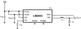
 Figure 11. LM2853 Example Circuit Schematic
Table 4. Bill of Materials for 5 V to 3.3 V Conversion
| ID | PART NUMBER | TYPE | SIZE | PARAMETERS | QTY | VENDOR |
|---|---|---|---|---|---|---|
| U1 | LM2853MH-3.3 | 3A Buck | HTSSOP-14 | 3.3 V | 1 | TI |
| CIN | GRM31CR60J476ME19 | Capacitor | 1206 | 47 µF | 1 | Murata |
| CBYP | GRM21BR71C105KA01 | Capacitor | 0805 | 1 µF | 1 | Murata |
| CSS | VJ0805Y222KXXA | Capacitor | 0603 | 2.2 nF | 1 | Vishay-Vitramon |
| LO | DO3316P-682 | Inductor | DO3316P | 6.8 µH | 1 | Coilcraft |
| CO | 594D127X06R3C2T | Capacitor | C Case | 120 μF (85 mΩ) | 1 | Vishay-Sprague |
Table 5. Bill of Materials for 3.3 V to 1.2 V Conversion
| ID | PART NUMBER | TYPE | SIZE | PARAMETERS | QTY | VENDOR |
|---|---|---|---|---|---|---|
| U1 | LM2853MH-1.2 | 3A Buck | HTSSOP-14 | 1.2 V | 1 | TI |
| CIN | GRM31CR60J476ME19 | Capacitor | 1206 | 47 µF | 1 | Murata |
| CBYP | GRM21BR71C105KA01 | Capacitor | 0805 | 1 µF | 1 | Murata |
| CSS | VJ0805Y222KXXA | Capacitor | 0603 | 2.2 nF | 1 | Vishay-Vitramon |
| LO | DO3316P-472 | Inductor | DO3316P | 4.7 μH | 1 | Coilcraft |
| CO | NOSD157M006R0070 | Capacitor | D Case | 150 μF (70 mΩ) | 1 | AVX |