JAJSAY1E March 2008 – October 2017 LM2854
PRODUCTION DATA.
- 1 特長
- 2 アプリケーション
- 3 概要
- 4 改訂履歴
- 5 Pin Configuration and Functions
- 6 Specifications
- 7 Detailed Description
-
8 Application and Implementation
- 8.1 Application Information
- 8.2
Typical Application
- 8.2.1 Design Requirements
- 8.2.2
Detailed Design Procedure
- 8.2.2.1 Input Filter Capacitor
- 8.2.2.2 AVIN Filtering Components
- 8.2.2.3 Soft-Start Capacitor
- 8.2.2.4 Tracking - Equal Soft-Start Time
- 8.2.2.5 Tracking - Equal Slew Rates
- 8.2.2.6 Enable and UVLO
- 8.2.2.7 Output Voltage Setting
- 8.2.2.8 Compensation Component Selection
- 8.2.2.9 Filter Inductor and Output Capacitor Selection
- 8.2.3 Application Curves
- 8.2.4 System Examples
- 9 Power Supply Recommendations
- 10Layout
- 11デバイスおよびドキュメントのサポート
- 12メカニカル、パッケージ、および注文情報
パッケージ・オプション
メカニカル・データ(パッケージ|ピン)
- PWP|16
サーマルパッド・メカニカル・データ
- PWP|16
発注情報
6.6 Typical Characteristics
Unless otherwise specified, the following conditions apply: VIN = PVIN = AVIN = EN = 5, TJ = 25°C.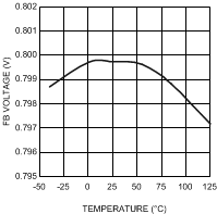 Figure 1. Feedback Voltage vs Temperature
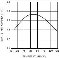 Figure 3. Soft Start Current vs Temperature
 Figure 5. Switching Frequency vs Temperature
 Figure 7. NMOS RDS(ON) vs Temperature
 Figure 9. Peak Current Limit vs Temperature
 Figure 11. IQ (disabled) vs VIN and Temperature, EN = 0 V
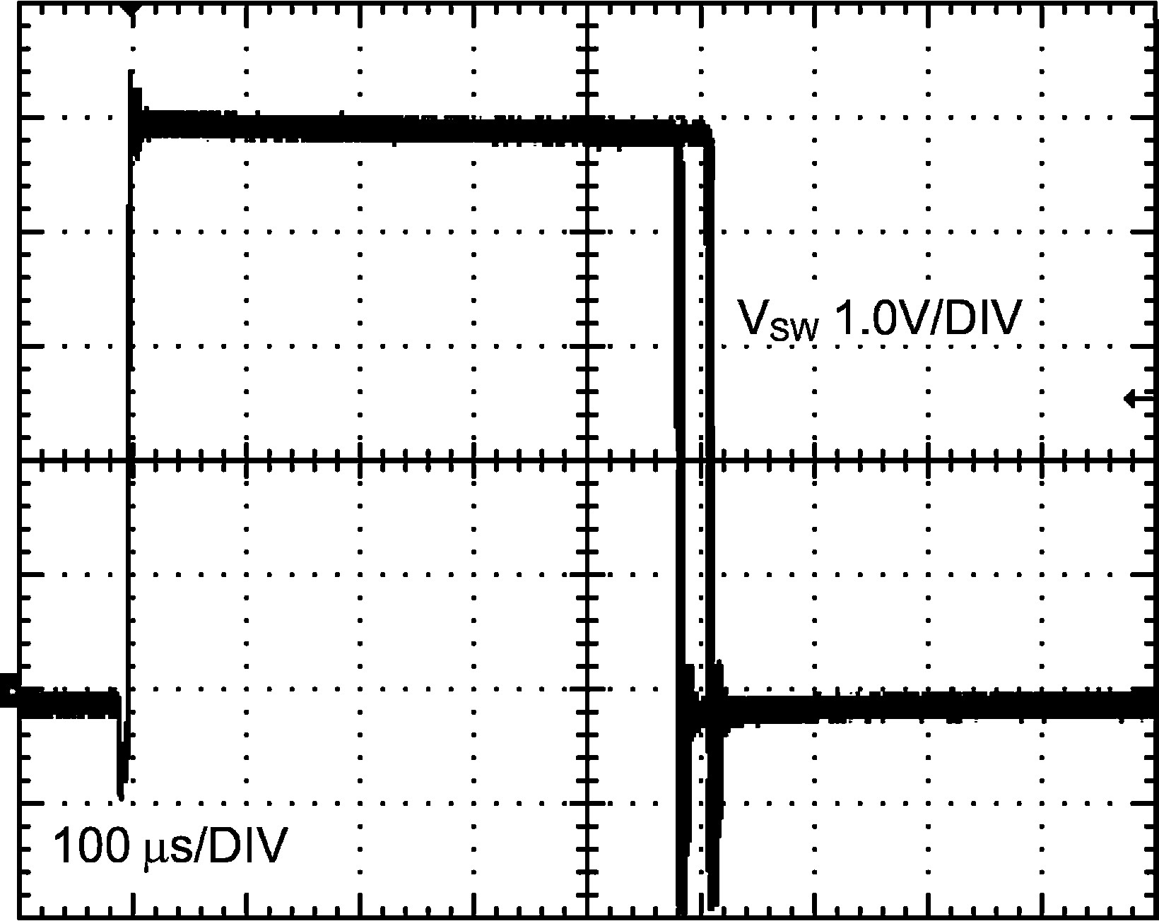 Figure 13. LM2854 500-kHz Switch Node Voltage (oscilloscope set at infinite persistence) VIN = 5 V, VOUT = 2.5 V, IOUT = 4 A
 Figure 2. UVLO Threshold vs Temperature
 Figure 4. Enable Threshold vs Temperature
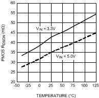 Figure 6. PMOS RDS(ON) vs Temperature
 Figure 8. IQ (operating) vs VIN and Temperature
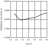 Figure 10. Feedback Voltage vs VIN
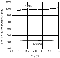 Figure 12. Switching Frequency vs VIN