JAJSAY1E March 2008 – October 2017 LM2854
PRODUCTION DATA.
- 1 特長
- 2 アプリケーション
- 3 概要
- 4 改訂履歴
- 5 Pin Configuration and Functions
- 6 Specifications
- 7 Detailed Description
-
8 Application and Implementation
- 8.1 Application Information
- 8.2
Typical Application
- 8.2.1 Design Requirements
- 8.2.2
Detailed Design Procedure
- 8.2.2.1 Input Filter Capacitor
- 8.2.2.2 AVIN Filtering Components
- 8.2.2.3 Soft-Start Capacitor
- 8.2.2.4 Tracking - Equal Soft-Start Time
- 8.2.2.5 Tracking - Equal Slew Rates
- 8.2.2.6 Enable and UVLO
- 8.2.2.7 Output Voltage Setting
- 8.2.2.8 Compensation Component Selection
- 8.2.2.9 Filter Inductor and Output Capacitor Selection
- 8.2.3 Application Curves
- 8.2.4 System Examples
- 9 Power Supply Recommendations
- 10Layout
- 11デバイスおよびドキュメントのサポート
- 12メカニカル、パッケージ、および注文情報
パッケージ・オプション
メカニカル・データ(パッケージ|ピン)
- PWP|16
サーマルパッド・メカニカル・データ
- PWP|16
発注情報
8.2.2.5 Tracking - Equal Slew Rates
Alternatively, the tracking feature can be used to have similar output voltage ramp rates. This is referred to as simultaneous start-up. In this case, the tracking resistors can be calculated using Equation 8.
Equation 8. 

and to ensure proper overdrive of the SS pin as calculated in Equation 9.
Equation 9. VOUT2< 0.8 VOUT1
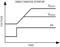
For the example case of VOUT1 = 5 V and VOUT2 = 2.5 V, with RT2 set to 33 kΩ as before, RT1 is calculated from the above equation to be 15.5 kΩ. A timing diagram for the case of equal slew rates is shown in Figure 18.
 Figure 18. Simplified Start-up Waveforms, Showing Tracking Used to Achieve Equal Slew Rates