JAJSAY1E March 2008 – October 2017 LM2854
PRODUCTION DATA.
- 1 特長
- 2 アプリケーション
- 3 概要
- 4 改訂履歴
- 5 Pin Configuration and Functions
- 6 Specifications
- 7 Detailed Description
-
8 Application and Implementation
- 8.1 Application Information
- 8.2
Typical Application
- 8.2.1 Design Requirements
- 8.2.2
Detailed Design Procedure
- 8.2.2.1 Input Filter Capacitor
- 8.2.2.2 AVIN Filtering Components
- 8.2.2.3 Soft-Start Capacitor
- 8.2.2.4 Tracking - Equal Soft-Start Time
- 8.2.2.5 Tracking - Equal Slew Rates
- 8.2.2.6 Enable and UVLO
- 8.2.2.7 Output Voltage Setting
- 8.2.2.8 Compensation Component Selection
- 8.2.2.9 Filter Inductor and Output Capacitor Selection
- 8.2.3 Application Curves
- 8.2.4 System Examples
- 9 Power Supply Recommendations
- 10Layout
- 11デバイスおよびドキュメントのサポート
- 12メカニカル、パッケージ、および注文情報
パッケージ・オプション
メカニカル・データ(パッケージ|ピン)
- PWP|16
サーマルパッド・メカニカル・データ
- PWP|16
発注情報
8.2.2.6 Enable and UVLO
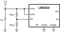
Using a resistor divider from VIN to EN as shown in the schematic diagram below, the input voltage at which the part begins switching can be increased above the normal input UVLO level as shown in Equation 10.
Equation 10. 

For example, suppose that the required input UVLO level is 3.69 V. Choosing REN2 = 10 kΩ, then we calculate REN1 = 20 kΩ.
 Figure 19. Simplified Schematic Showing Use of EN as an Input UVLO
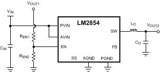
Alternatively, the EN pin can be driven from another voltage source to cater for system sequencing requirements commonly found in FPGA and other multi-rail applications. The following schematic shows an LM2854 that is sequenced to start based on the voltage level of a master system rail.
 Figure 20. Simplified Schematic Showing EN Used to Cascade Power Supply Start-up