SNVS093G June 1999 – May 2015 LM2990
PRODUCTION DATA.
- 1 Features
- 2 Applications
- 3 Description
- 4 Revision History
- 5 Pin Configuration and Functions
- 6 Specifications
- 7 Detailed Description
- 8 Application and Implementation
- 9 Power Supply Recommendations
- 10Layout
- 11Device and Documentation Support
- 12Mechanical, Packaging, and Orderable Information
7 Detailed Description
7.1 Overview
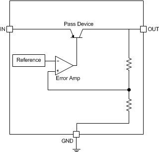
The LM2990 is a three-terminal, low dropout, 1-A negative voltage regulator available with fixed output voltages of −5, −5.2, −12, and −15 V. The LM2990 is a negative power supply ideally suited for a dual-supply system when using together with LM2940 series. The device may also be used as a fixed or adjustable current sink load.
7.2 Functional Block Diagram

7.3 Feature Description
7.3.1 Fixed Output-Voltage Options
The LM2990 provides 4 fixed output options: −5 V, −5.2 V, −12 V, and −15 V. Output voltage accuracy is ensured to ±5% over load and temperature extremes.
7.3.2 Low Dropout Voltage
Generally speaking, the dropout voltage (VDO) refers to the voltage difference between the IN pin and the OUT pin when the PNP pass element is fully on and is characterized by the classic Collector-to-Emitter saturation voltage, VCE(SAT). VDO indirectly specifies a minimum input voltage above the nominal programmed output voltage at which the output voltage is expected to remain within its accuracy boundary.
7.3.3 Short Circuit Protection (Current Limit)
The internal current limit circuit is used to protect the LDO against high-load current faults or shorting events. The LDO is not designed to operate in a steady-state current limit. During a current-limit event, the LDO sources constant current. Therefore, the output voltage falls when load impedance decreases. Note also that if a current limit occurs and the resulting output voltage is low, excessive power may be dissipated across the LDO, resulting in a thermal shutdown of the output. A fold back feature limits the short-circuit current to protect the regulator from damage under all load conditions. If OUT is forced below 0 V before EN goes high, and the load current required exceeds the fold back current limit, the device may not start up correctly.
7.3.4 Thermal Protection
The device contains a thermal shutdown protection circuit to turn off the output current when excessive heat is dissipated in the LDO. The thermal time-constant of the semiconductor die is fairly short, and thus the output cycles on and off at a high rate when thermal shutdown is reached until the power dissipation is reduced. The internal protection circuitry of the device is designed to protect against thermal overload conditions. The circuitry is not intended to replace proper heat sinking. Continuously running the device into thermal shutdown degrades its reliability.
7.4 Device Functional Modes
7.4.1 Operation with VOUT(TARGET) –5 V ≥ VIN > –26 V
The device operates if the input voltage is within VOUT(TARGET) –5 V to –26 V range. At input voltages beyond the VIN requirement, the devices do not operate correctly, and output voltage may not reach target value.