JAJSDE1 June 2017 LM317-N-MIL
PRODUCTION DATA.
- 1 特長
- 2 アプリケーション
- 3 概要
- 4 改訂履歴
- 5 Pin Configuration and Functions
- 6 Specifications
- 7 Detailed Description
-
8 Application and Implementation
- 8.1 Application Information
- 8.2
Typical Applications
- 8.2.1 1.25-V to 25-V Adjustable Regulator
- 8.2.2 5-V Logic Regulator With Electronic Shutdown
- 8.2.3 Slow Turnon 15-V Regulator
- 8.2.4 Adjustable Regulator With Improved Ripple Rejection
- 8.2.5 High Stability 10-V Regulator
- 8.2.6 High-Current Adjustable Regulator
- 8.2.7 Emitter-Follower Current Amplifier
- 8.2.8 1-A Current Regulator
- 8.2.9 Common-Emitter Amplifier
- 8.2.10 Low-Cost 3-A Switching Regulator
- 8.2.11 Current-Limited Voltage Regulator
- 8.2.12 Adjusting Multiple On-Card Regulators With Single Control
- 8.2.13 AC Voltage Regulator
- 8.2.14 12-V Battery Charger
- 8.2.15 Adjustable 4-A Regulator
- 8.2.16 Current-Limited 6-V Charger
- 8.2.17 Digitally Selected Outputs
- 9 Power Supply Recommendations
- 10Layout
- 11デバイスおよびドキュメントのサポート
- 12メカニカル、パッケージ、および注文情報
5 Pin Configuration and Functions
NDS Metal Can Package
2-Pin TO-3
Bottom View

Case is Output
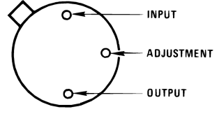
NDT Metal Can Package
3-Pin TO
Bottom View

Case is Output
Pin Functions, Metal Can Packages
| PIN | I/O | DESCRIPTION | ||
|---|---|---|---|---|
| NAME | TO-3 | TO | ||
| ADJ | 1 | 2 | — | Adjust pin |
| VOUT | CASE | 3, CASE | O | Output voltage pin for the regulator |
| VIN | 2 | 1 | I | Input voltage pin for the regulator |
KTT Surface-Mount Package
3-Pin DDPAK/TO-263
Top View

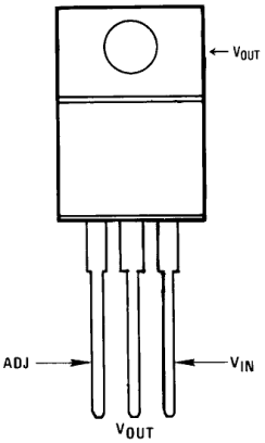
NDE Plastic Package
3-Pin TO-220
Front View

DCY Surface-Mount Package
4-Pin SOT-223
Top View

NDP Surface-Mount Package
3-Pin TO-252
Front View

Pin Functions
| PIN | I/O | DESCRIPTION | ||||
|---|---|---|---|---|---|---|
| NAME | TO-263 | TO-220 | SOT-223 | TO-252 | ||
| ADJ | 1 | 1 | 1 | 1 | — | Adjust pin |
| VOUT | 2, TAB | 2, TAB | 2, 4 | 2, TAB | O | Output voltage pin for the regulator |
| VIN | 3 | 3 | 3 | 3 | I | Input voltage pin for the regulator |