JAJSDE1 June 2017 LM317-N-MIL
PRODUCTION DATA.
- 1 特長
- 2 アプリケーション
- 3 概要
- 4 改訂履歴
- 5 Pin Configuration and Functions
- 6 Specifications
- 7 Detailed Description
-
8 Application and Implementation
- 8.1 Application Information
- 8.2
Typical Applications
- 8.2.1 1.25-V to 25-V Adjustable Regulator
- 8.2.2 5-V Logic Regulator With Electronic Shutdown
- 8.2.3 Slow Turnon 15-V Regulator
- 8.2.4 Adjustable Regulator With Improved Ripple Rejection
- 8.2.5 High Stability 10-V Regulator
- 8.2.6 High-Current Adjustable Regulator
- 8.2.7 Emitter-Follower Current Amplifier
- 8.2.8 1-A Current Regulator
- 8.2.9 Common-Emitter Amplifier
- 8.2.10 Low-Cost 3-A Switching Regulator
- 8.2.11 Current-Limited Voltage Regulator
- 8.2.12 Adjusting Multiple On-Card Regulators With Single Control
- 8.2.13 AC Voltage Regulator
- 8.2.14 12-V Battery Charger
- 8.2.15 Adjustable 4-A Regulator
- 8.2.16 Current-Limited 6-V Charger
- 8.2.17 Digitally Selected Outputs
- 9 Power Supply Recommendations
- 10Layout
- 11デバイスおよびドキュメントのサポート
- 12メカニカル、パッケージ、および注文情報
6 Specifications
6.1 Absolute Maximum Ratings
over operating free-air temperature range (unless otherwise noted)(1)(2)| MIN | MAX | UNIT | ||
|---|---|---|---|---|
| Power dissipation | Internally Limited | |||
| Input-output voltage differential | −0.3 | 40 | V | |
| Lead temperature | Metal package (soldering, 10 seconds) | 300 | °C | |
| Plastic package (soldering, 4 seconds) | 260 | °C | ||
| Storage temperature, Tstg | −65 | 150 | °C | |
(1) Stresses beyond those listed under Absolute Maximum Ratings may cause permanent damage to the device. These are stress ratings only, which do not imply functional operation of the device at these or any other conditions beyond those indicated under Recommended Operating Conditions. Exposure to absolute-maximum-rated conditions for extended periods may affect device reliability.
(2) If Military/Aerospace specified devices are required, please contact the Texas Instruments Sales Office/Distributors for availability and specifications.
6.2 ESD Ratings
| VALUE | UNIT | |||
|---|---|---|---|---|
| V(ESD) | Electrostatic discharge | Human-body model (HBM)(1) | ±3000 | V |
(1) Manufacturing with less than 500-V HBM is possible with the necessary precautions. Pins listed as ±3000 V may actually have higher performance.
6.3 Recommended Operating Conditions
over operating free-air temperature range (unless otherwise noted)| MIN | MAX | UNIT | ||
|---|---|---|---|---|
| Operating temperature (LM117) | −55 | 150 | °C | |
| Operating temperature (LM317-N) | 0 | 125 | °C | |
6.4 Thermal Information
| THERMAL METRIC(1)(2) | LM317-N | UNIT | |||||
|---|---|---|---|---|---|---|---|
| KTT (TO-263) |
NDE (TO-220) |
DCY (SOT-223) |
NDT (TO) |
NDP (TO-252) |
|||
| 3 PINS | 3 PINS | 4 PINS | 3 PINS | 3 PINS | |||
| RθJA | Junction-to-ambient thermal resistance | 41.0 | 23.3 | 59.6 | 186(3) | 54 | °C/W |
| RθJC(top) | Junction-to-case (top) thermal resistance | 43.6 | 16.2 | 39.3 | 21 | 51.3 | °C/W |
| RθJB | Junction-to-board thermal resistance | 23.6 | 4.9 | 8.4 | — | 28.6 | °C/W |
| ψJT | Junction-to-top characterization parameter | 10.4 | 2.7 | 1.8 | — | 3.9 | °C/W |
| ψJB | Junction-to-board characterization parameter | 22.6 | 4.9 | 8.3 | — | 28.1 | °C/W |
| RθJC(bot) | Junction-to-case (bottom) thermal resistance | 0.9 | 1.1 | — | — | 0.9 | °C/W |
(1) For more information about traditional and new thermal metrics, see the Semiconductor and IC Package Thermal Metrics application report, SPRA953.
(2) When surface mount packages are used (SOT-223, TO-252), the junction to ambient thermal resistance can be reduced by increasing the PCB copper area that is thermally connected to the package. See Heatsink Requirements for heatsink techniques.
(3) No heatsink
6.5 Electrical Characteristics(1)
Some specifications apply over full Operating Temperature Range as noted. Unless otherwise specified, TJ = 25°C, VIN − VOUT = 5 V, and IOUT = 10 mA.| PARAMETER | TEST CONDITIONS | MIN | TYP | MAX | UNIT | |
|---|---|---|---|---|---|---|
| Reference voltage | TJ = 25°C | 1.25 | V | |||
| 3 V ≤ (VIN − VOUT) ≤ 40 V, 10 mA ≤ IOUT ≤ IMAX(1) (over Full Operating Temperature Range) |
1.2 | 1.25 | 1.3 | V | ||
| Line regulation | 3V ≤ (VIN − VOUT) ≤ 40 V(2) | TJ = 25°C | 0.01 | 0.04 | %/V | |
| (over full operating temperature range) | 0.02 | 0.07 | ||||
| Load regulation | 10 mA ≤ IOUT ≤ IMAX(1)(2) | TJ = 25°C | 0.1% | 0.5% | ||
| (over full operating temperature range) | 0.3% | 1.5% | ||||
| Thermal regulation | 20-ms pulse | 0.04 | 0.07 | %/W | ||
| Adjustment pin current | (over full operating temperature range) | 50 | 100 | μA | ||
| Adjustment pin current change | 10 mA ≤ IOUT ≤ IMAX(1)
3V ≤ (VIN − VOUT) ≤ 40V |
(over full operating temperature range) | 0.2 | 5 | μA | |
| Temperature stability | TMIN ≤ TJ ≤ TMAX | (over full operating temperature range) | 1% | |||
| Minimum load current | (VIN − VOUT) = 40 V | (over full operating temperature range) | 3.5 | 10 | mA | |
| Current limit | (VIN − VOUT) ≤ 15 V | TO-3, TO-263 Packages (over full operating temperature range) | 1.5 | 2.2 | 3.4 | A |
| SOT-223, TO-220 Packages (over full operating temperature range) | 1.5 | 2.2 | 3.4 | |||
| TO, TO-252 Package (over full operating temperature range) | 0.5 | 0.8 | 1.8 | |||
| (VIN − VOUT) = 40 V | TO-3, TO-263 packages | 0.15 | 0.4 | A | ||
| SOT-223, TO-220 packages | 0.15 | 0.4 | ||||
| TO, TO-252 package | 0.075 | 0.2 | ||||
| RMS output noise, % of VOUT | 10 Hz ≤ f ≤ 10 kHz | 0.003% | ||||
| Ripple rejection ratio | VOUT = 10 V, f = 120 Hz, CADJ = 0 μF (over full operating temperature range) | 65 | dB | |||
| VOUT = 10V, f = 120 Hz, CADJ = 10 μF (over full operating temperature range) | 66 | 80 | dB | |||
| Long-term stability | TJ = 125°C, 1000 hrs | 0.3% | 1% | |||
(1) IMAX = 1.5 A for the NDS (TO-3), NDE (TO-220), and KTT (TO-263) packages. IMAX = 1.0 A for the DCY (SOT-223) package.
IMAX = 0.5 A for the NDT (TO) and NDP (TO-252) packages. Device power dissipation (PD) is limited by ambient temperature (TA), device maximum junction temperature (TJ), and package thermal resistance (θJA). The maximum allowable power dissipation at any temperature is : PD(MAX) = ((TJ(MAX) – TA) / θJA). All Min. and Max. limits are ensured to TI's Average Outgoing Quality Level (AOQL).
IMAX = 0.5 A for the NDT (TO) and NDP (TO-252) packages. Device power dissipation (PD) is limited by ambient temperature (TA), device maximum junction temperature (TJ), and package thermal resistance (θJA). The maximum allowable power dissipation at any temperature is : PD(MAX) = ((TJ(MAX) – TA) / θJA). All Min. and Max. limits are ensured to TI's Average Outgoing Quality Level (AOQL).
(2) Regulation is measured at a constant junction temperature, using pulse testing with a low duty cycle. Changes in output voltage due to heating effects are covered under the specifications for thermal regulation.
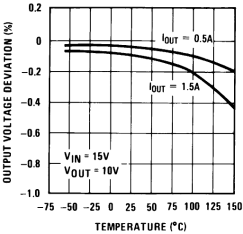
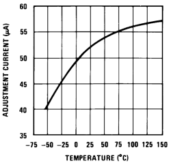
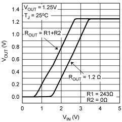
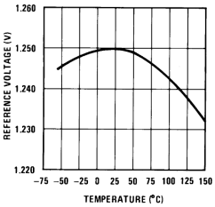
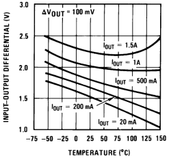
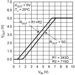
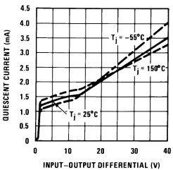
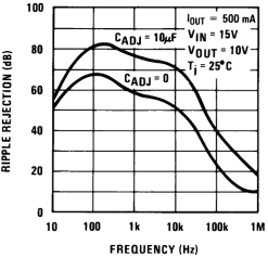
6.6 Typical Characteristics
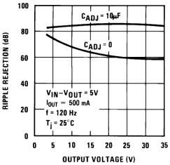
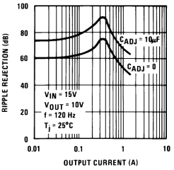
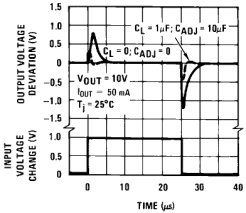
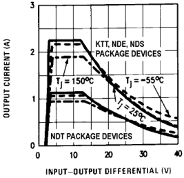
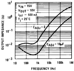
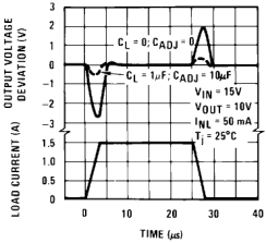
Output Capacitor = 0 μF, unless otherwise noted.