JAJSDE2 June 2017 LM317HV-MIL
PRODUCTION DATA.
- 1 特長
- 2 アプリケーション
- 3 概要
- 4 改訂履歴
- 5 Pin Configuration and Functions
- 6 Specifications
- 7 Detailed Description
-
8 Application and Implementation
- 8.1 Application Information
- 8.2
Typical Applications
- 8.2.1 1.25-V to 45-V High Voltage Adjustable Regulator
- 8.2.2 Digitally Selected Outputs
- 8.2.3 Logic Regulator (5-V) With Electronic Shutdown
- 8.2.4 Slow Turnon 15-V Regulator
- 8.2.5 Adjustable Regulator With Improved Ripple Rejection
- 8.2.6 High Stability 10-V Regulator
- 8.2.7 High Current Adjustable Regulator
- 8.2.8 Emitter Follower Current Amplifier
- 8.2.9 1-A Current Regulator
- 8.2.10 Common Emitter Amplifier
- 8.2.11 Low-Cost, 3-A Switching Regulator
- 8.2.12 Adjustable Multiple On-Card Regulators With Single Control
- 8.2.13 AC Voltage Regulator
- 8.2.14 12-V Battery Charger
- 8.2.15 Adjustable 4-A Regulator
- 8.2.16 Current Limited 6-V Charger
- 9 Power Supply Recommendations
- 10Layout
- 11デバイスおよびドキュメントのサポート
- 12メカニカル、パッケージ、および注文情報
8 Application and Implementation
NOTE
Information in the following applications sections is not part of the TI component specification, and TI does not warrant its accuracy or completeness. TI’s customers are responsible for determining suitability of components for their purposes. Customers should validate and test their design implementation to confirm system functionality.
8.1 Application Information
The LM317HV-MIL is a high voltage input capable linear regulator with overload protection. Due to its wide input voltage range, the LM317HV-MIL serves a variety of applications and provides a precise voltage regulation with low dropout across a wide output voltage and load current range. The device regulates a constant 1.25 V between VOUT and ADJ, so placing a fixed resistor between these pins provides a constant current regulation. Capacitors at the input help filter the input power supply, while the output capacitors aid in transient response stability. A bypass capacitor can be placed between ADJ pin and ground (across R2) to improve ripple rejection.
8.2 Typical Applications
8.2.1 1.25-V to 45-V High Voltage Adjustable Regulator
The device can be used as an adjustable regulator to allow a variety of output voltages for high voltage applications. By using an adjustable R2 resistor, a variety of output voltages can be made possible as shown in Figure 16.
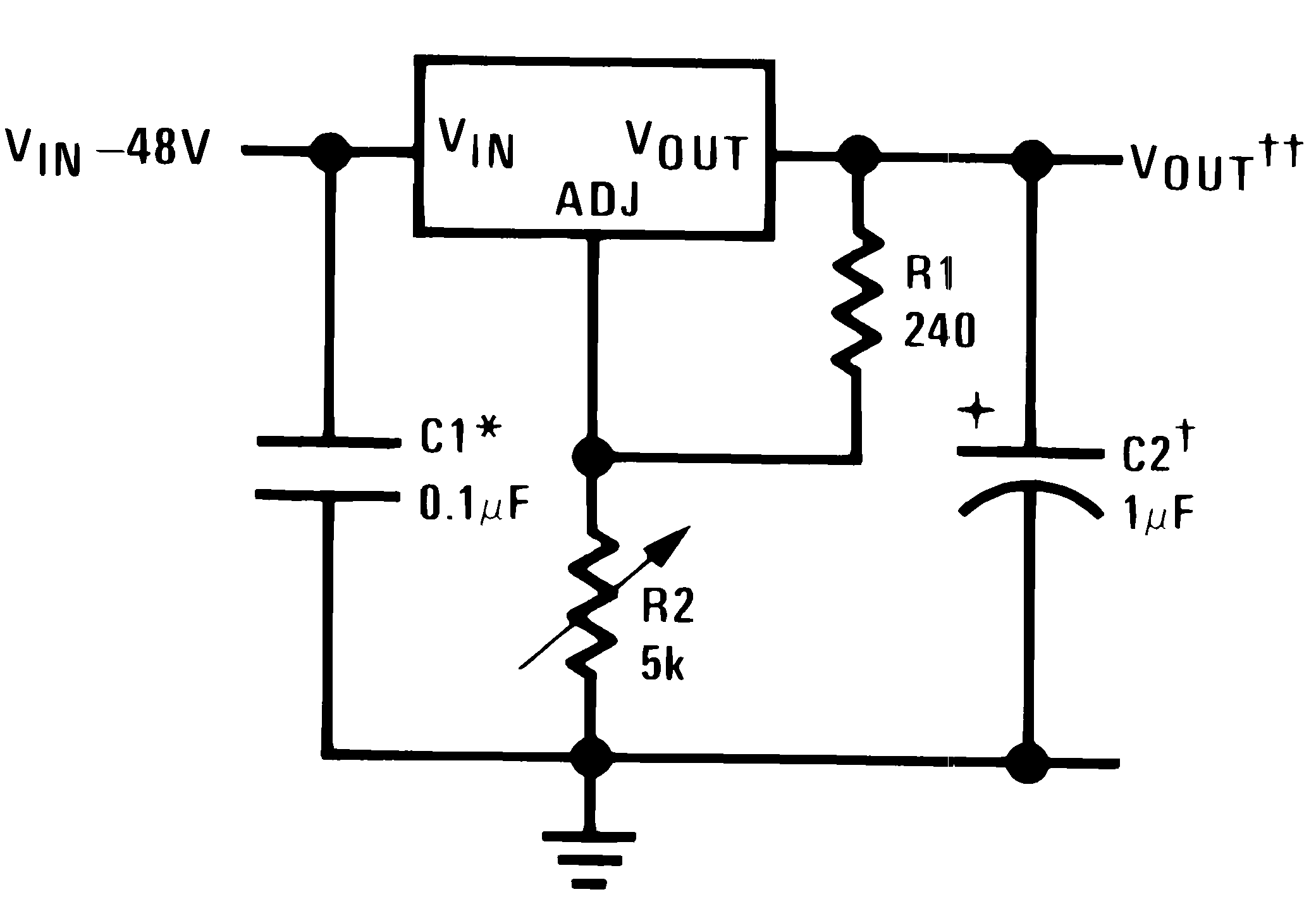
†Optional—improves transient response. Output capacitors in the range of 1 μF to 1000 μF of aluminum or tantalum electrolytic
are commonly used to provide improved output impedance and rejection of transients.
*Needed if device is more than 6 inches from filter capacitors.
††

8.2.1.1 Design Requirements
The device component count is very minimal, employing two resistors as part of a voltage divider circuit and an output capacitor for load regulation. An input capacitor is needed if the device is more than 6 inches from filter capacitors. An optional bypass capacitor across R2 can also be used to improve PSRR.
8.2.1.2 Detailed Design Procedure
The output voltage is set based on the selection of the two resistors, R1 and R2, as shown in Figure 16. For details on capacitor selection, refer to External Capacitors.
8.2.1.3 Application Curve
As shown in Figure 17, the maximum output current capability is limited by the input-output voltage differential, package type, and junction temperature.
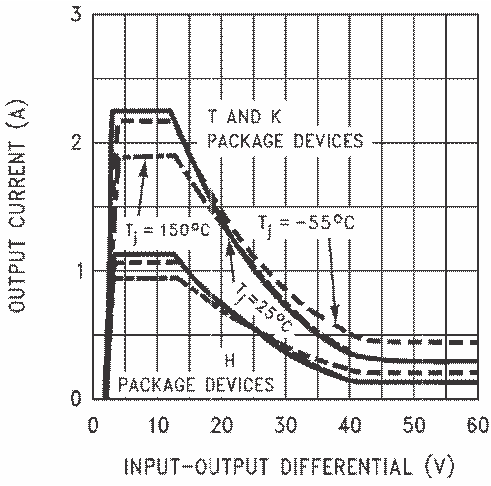 Figure 17. Current Limit
8.2.2 Digitally Selected Outputs
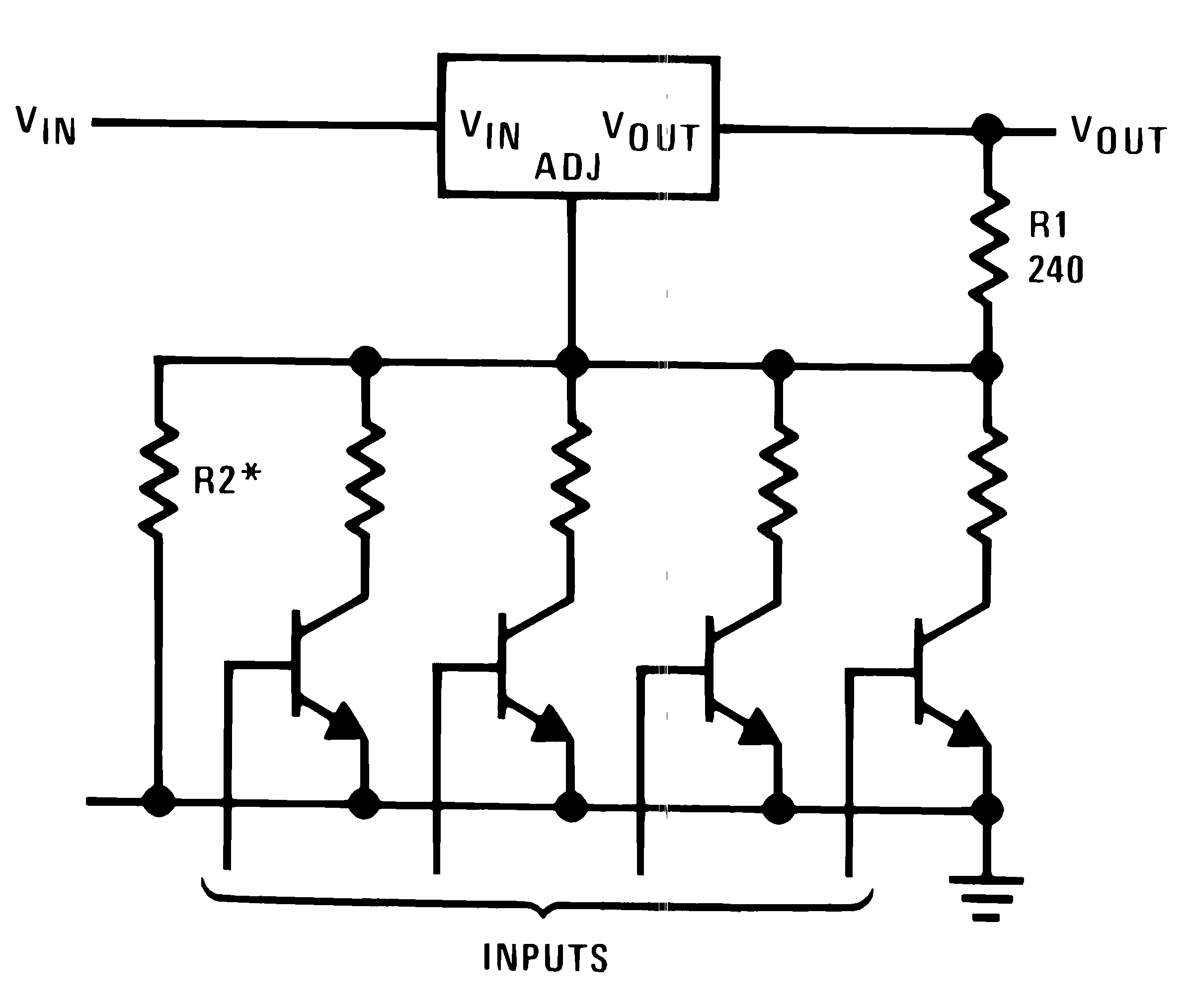
Figure 18 shows a digitally selectable output voltage. In its default state, all transistors are off and the output voltage is set based on R1 and R2. By driving certain transistors, the associated resistor is connected in parallel to R2, modifying the output voltage of the regulator.
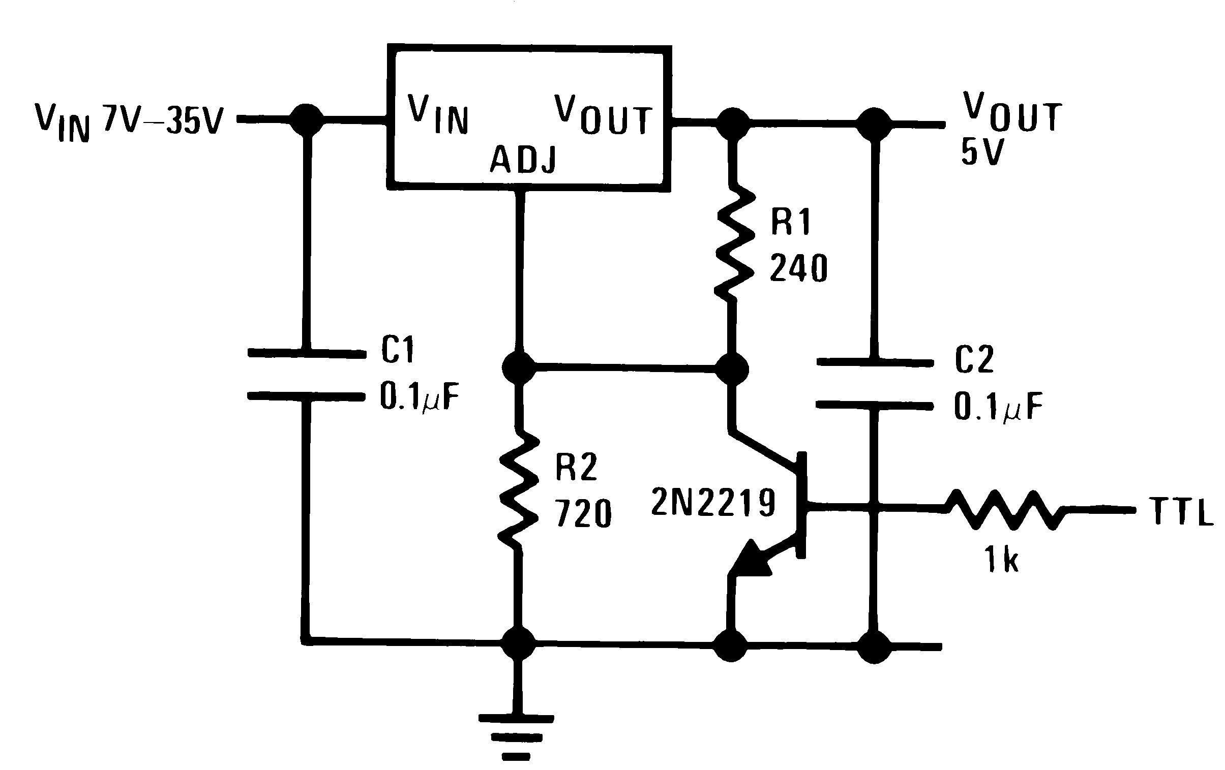
8.2.3 Logic Regulator (5-V) With Electronic Shutdown
A variation of the 5-V output regulator application uses the LM317HV-MIL along with an NPN transistor to provide shutdown control. The NPN will either block or sink the current from the ADJ pin by responding to the TTL pin logic. When TTL is pulled high, the NPN is on and pulls the ADJ pin to GND, and the device outputs about 1.25 V. When TTL is pulled low, the NPN is off and the regulator outputs according to the programmed adjustable voltage.
NOTE:
*Min. output ≈ 1.2 V8.2.4 Slow Turnon 15-V Regulator
An application of LM317HV-MIL includes a PNP transistor with a capacitor to implement slow turnon functionality. As VIN rises, the PNP sinks current from the ADJ rail. The output voltage at start-up is the addition of the 1.25-V reference plus the drop across the base to emitter. While this is happening, the capacitor begins to charge and eventually opens the PNP. At this point, the device functions normally, regulating the output at 15 V. A diode is placed between C1 and VOUT to provide a path for the capacitor to discharge. Such controlled turnon is useful for limiting the in-rush current.
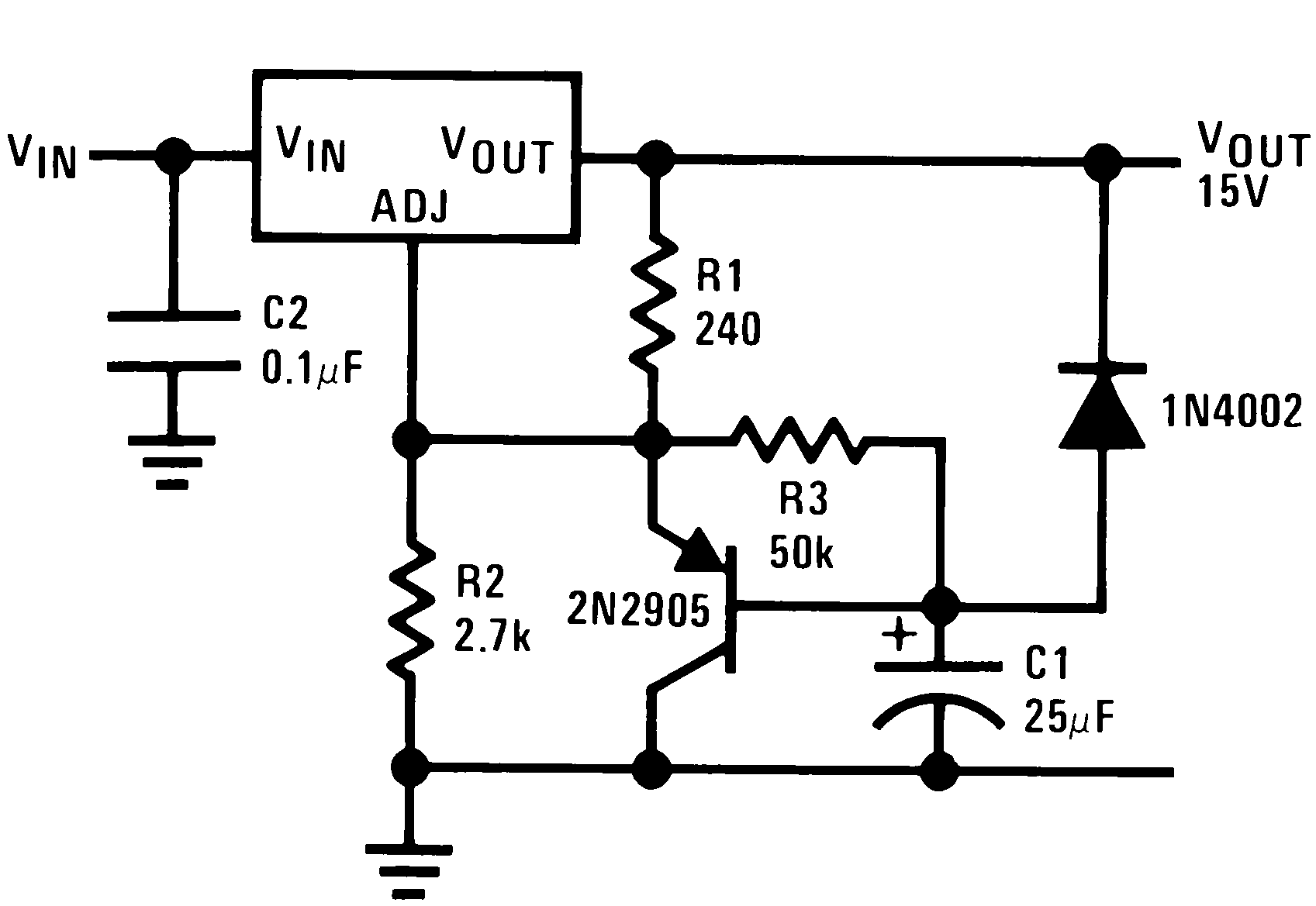 Figure 20. Slow Turnon 15-V Regulator
8.2.5 Adjustable Regulator With Improved Ripple Rejection
To improve ripple rejection, a capacitor is used to bypass the ADJ pin to GND. This is used to smooth output ripple by cleaning the feedback path and stopping unnecessary noise from being fed back into the device, propagating the noise.
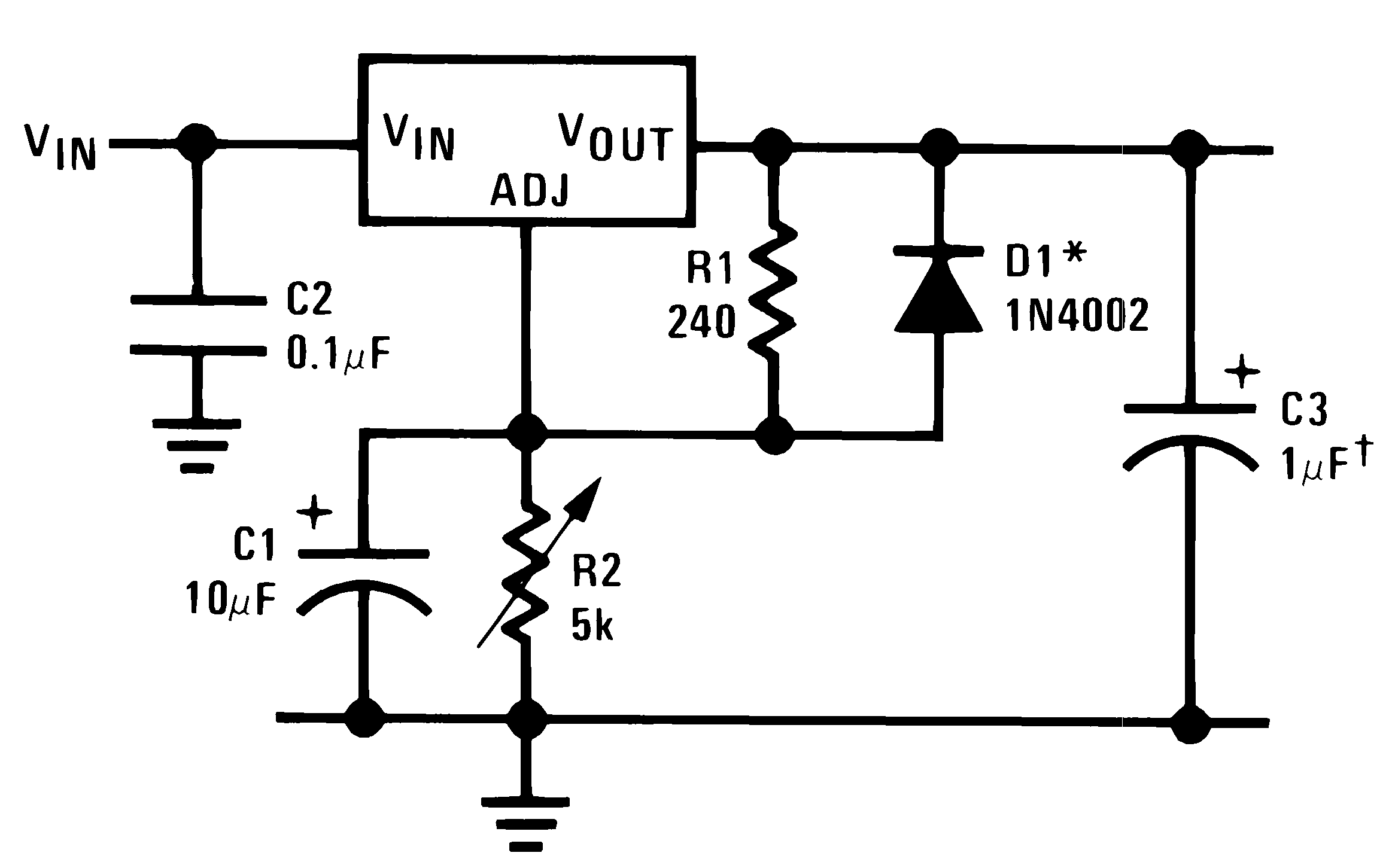
*Discharges C1 if output is shorted to ground
8.2.6 High Stability 10-V Regulator
Using a high-stability shunt voltage reference in the feedback path, such as the LM329, provides damping necessary for a stable, low noise output.
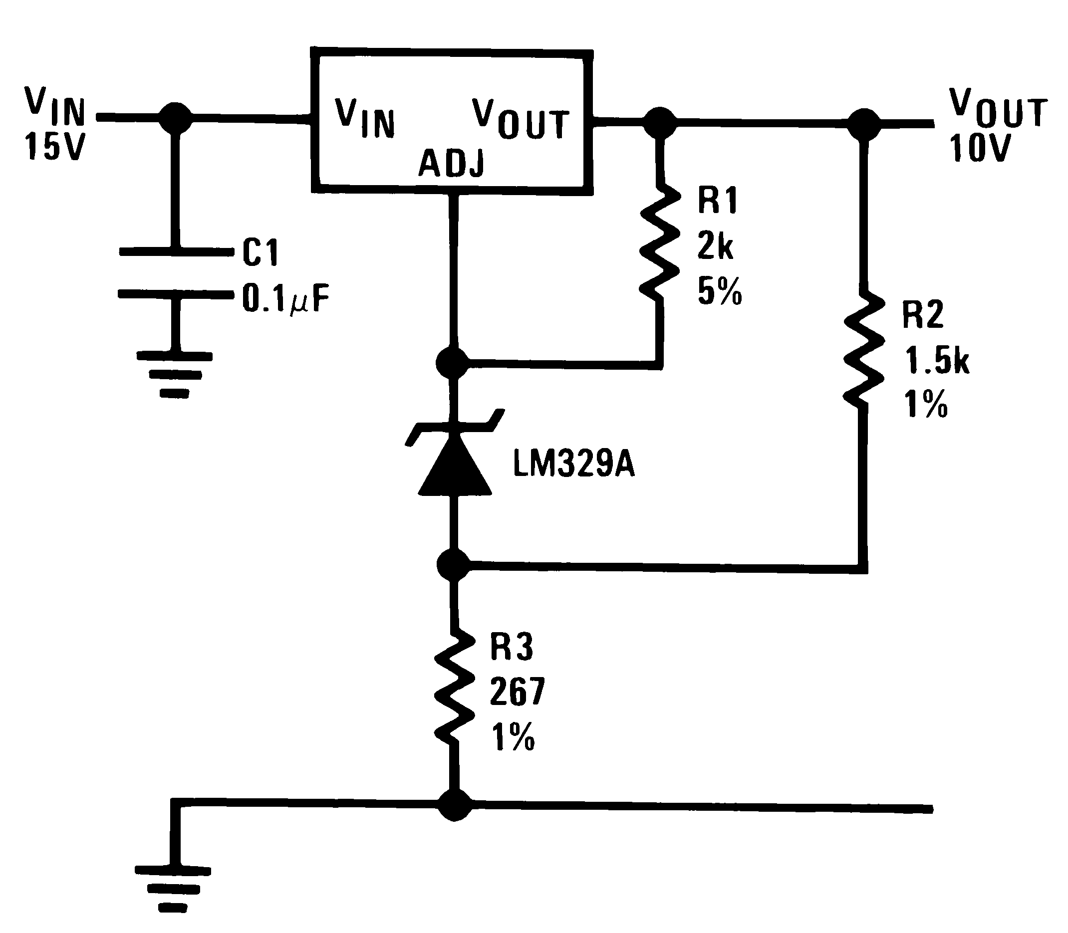 Figure 22. High Stability 10-V Regulator
8.2.7 High Current Adjustable Regulator
Using the LM195 power transistor in parallel with the LM317HV-MIL can increase the maximum possible output load current. Sense resistor R1 provides the 0.6 V across base to emitter to turn on the PNP. This on switch allows current to flow, and the voltage drop across R3 drives three LM195 power transistors designed to carry an excess of 1 A each. Note the selection of R1 determines a minimum load current for the PNP to turn on. The higher the resistor value, the lower the load current must be before the transistors turn on.
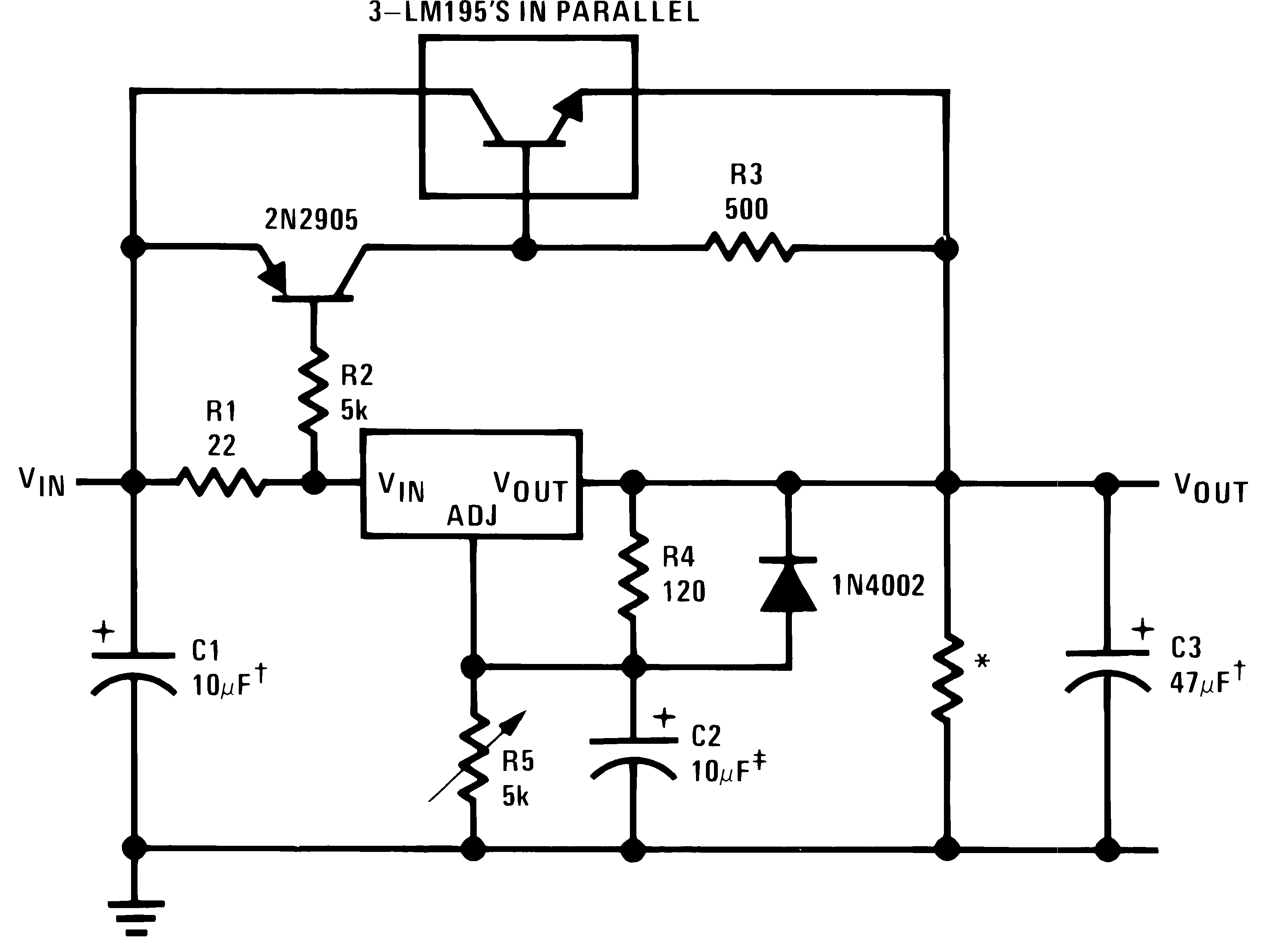
*Minimum load current = 30 mA
‡Optional—improves ripple rejection
8.2.8 Emitter Follower Current Amplifier
The device is used as a constant current source in this emitter follower circuit. The LM195 power transistor is being used as a current gain amplifier, boosting the INPUT current. The device provides a stable current bias than just using a resistor.
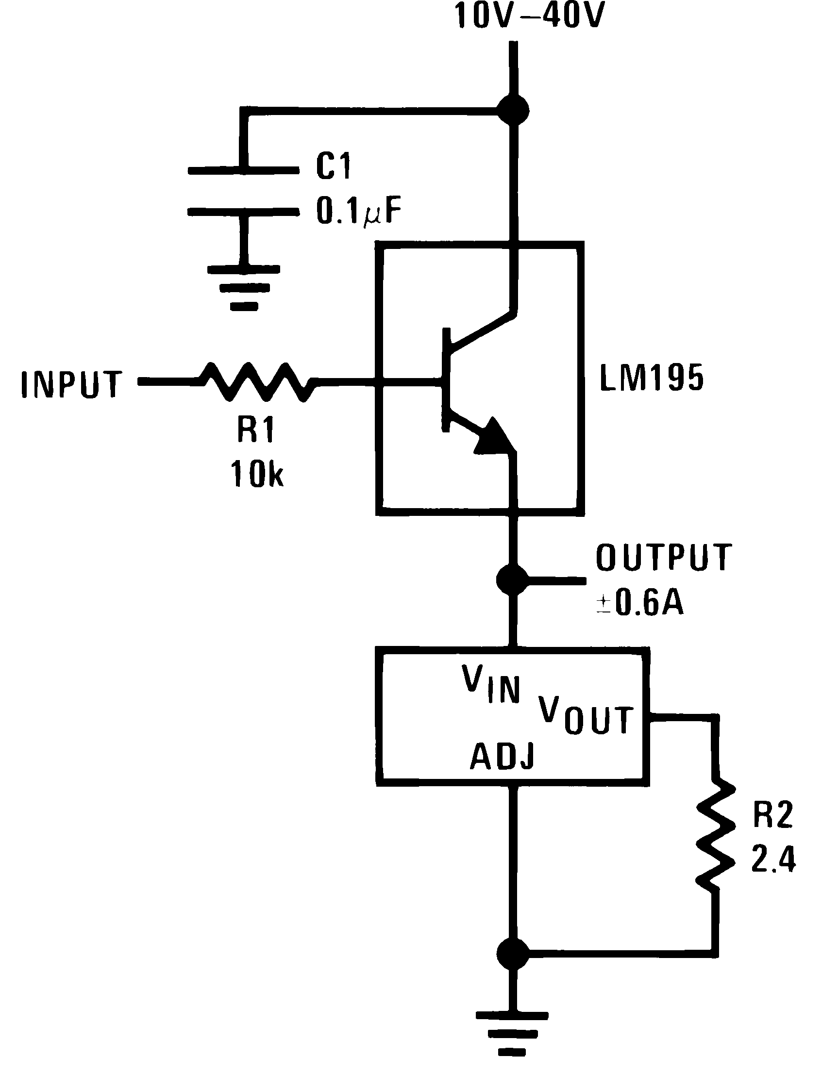 Figure 24. Emitter Follower Current Amplifier
8.2.9 1-A Current Regulator
A simple, fixed-current regulator can be made by placing a resistor between the VOUT and ADJ pins of the LM317HV-MIL. By regulating a constant 1.25 V between these two terminals, a constant current is delivered to the load.
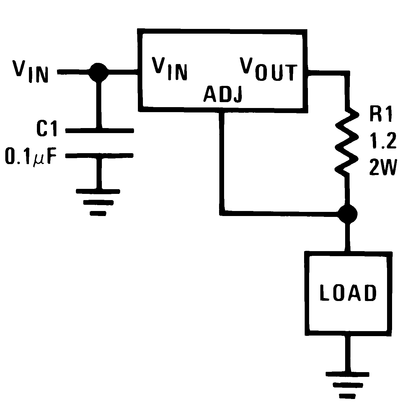 Figure 25. 1-A Current Regulator
8.2.10 Common Emitter Amplifier
Sometimes it is necessary to use a power transistor for high current gain. In this case, the LM317HV-MIL provides constant current at the collector of the LM195 in this common emitter application. The 1.25-V reference between VOUT and ADJ is maintained across the 2.4-Ω resistor, providing about 500-mA constant bias current into the collector of the LM195.
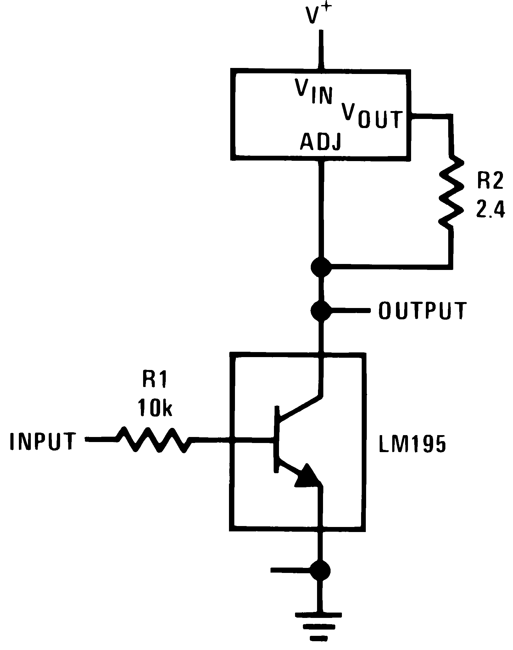 Figure 26. Common Emitter Amplifier
8.2.11 Low-Cost, 3-A Switching Regulator
The LM317HV-MIL can be used in a switching buck regulator application in cost-sensitive applications that require high efficiency. The switch node above D1 oscillates between ground and VIN, as the voltage across sense resistor R1 drives the power transistor on and off. This circuit exhibits self-oscillating behavior by negative feedback through R6 and C3 to the ADJ pin of the LM317HV-MIL.
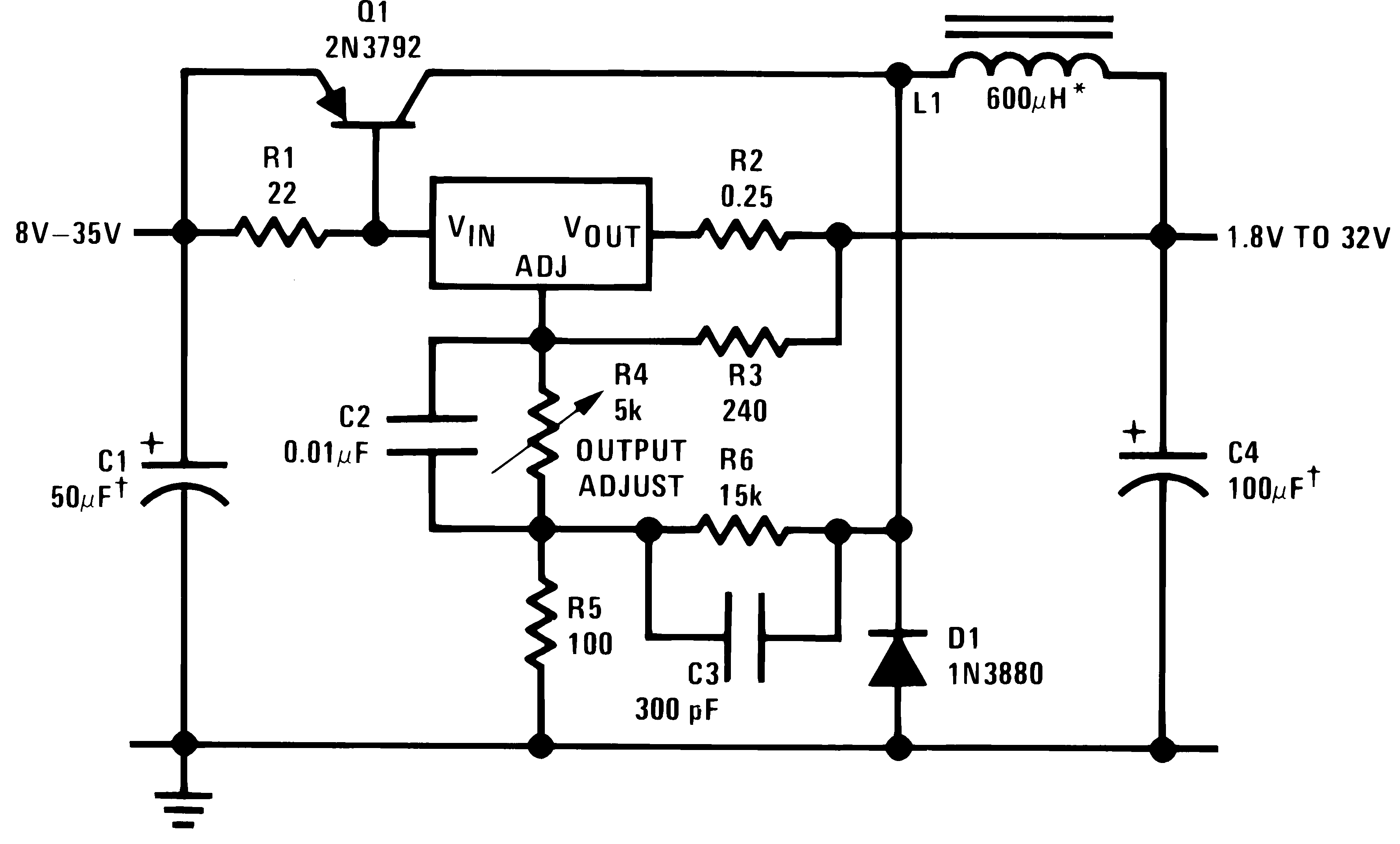
*Core—Arnold A-254168-2 60 turns
8.2.12 Adjustable Multiple On-Card Regulators With Single Control
This application shows how multiple LM317HV-MIL regulators can be controlled by setting one resistor. Because each device maintains the reference voltage of about 1.25 V between its VOUT and ADJ pins, we can connect each ADJ rail to a single resistor, setting the same output voltage across all devices. This allows for independent outputs, each responding to its corresponding input only. Designers must also consider that by the nature of the circuit, changes to R1 and R2 affect all regulators.

NOTE:
*All outputs within ±100 mV†Minimum load—10 mA
8.2.13 AC Voltage Regulator
In Figure 29, the top regulator is +6 V above the bottom regulator. It is clear that when the input rises above +6 V plus the dropout voltage, only the top LM317HV-MIL regulates +6 V at the output. When the input falls below –6 V minus the dropout voltage, only the bottom LM317HV-MIL regulates –6 V at the output. For regions where the output is not clipped, there is no regulation taking place, so we see the output follow the input.
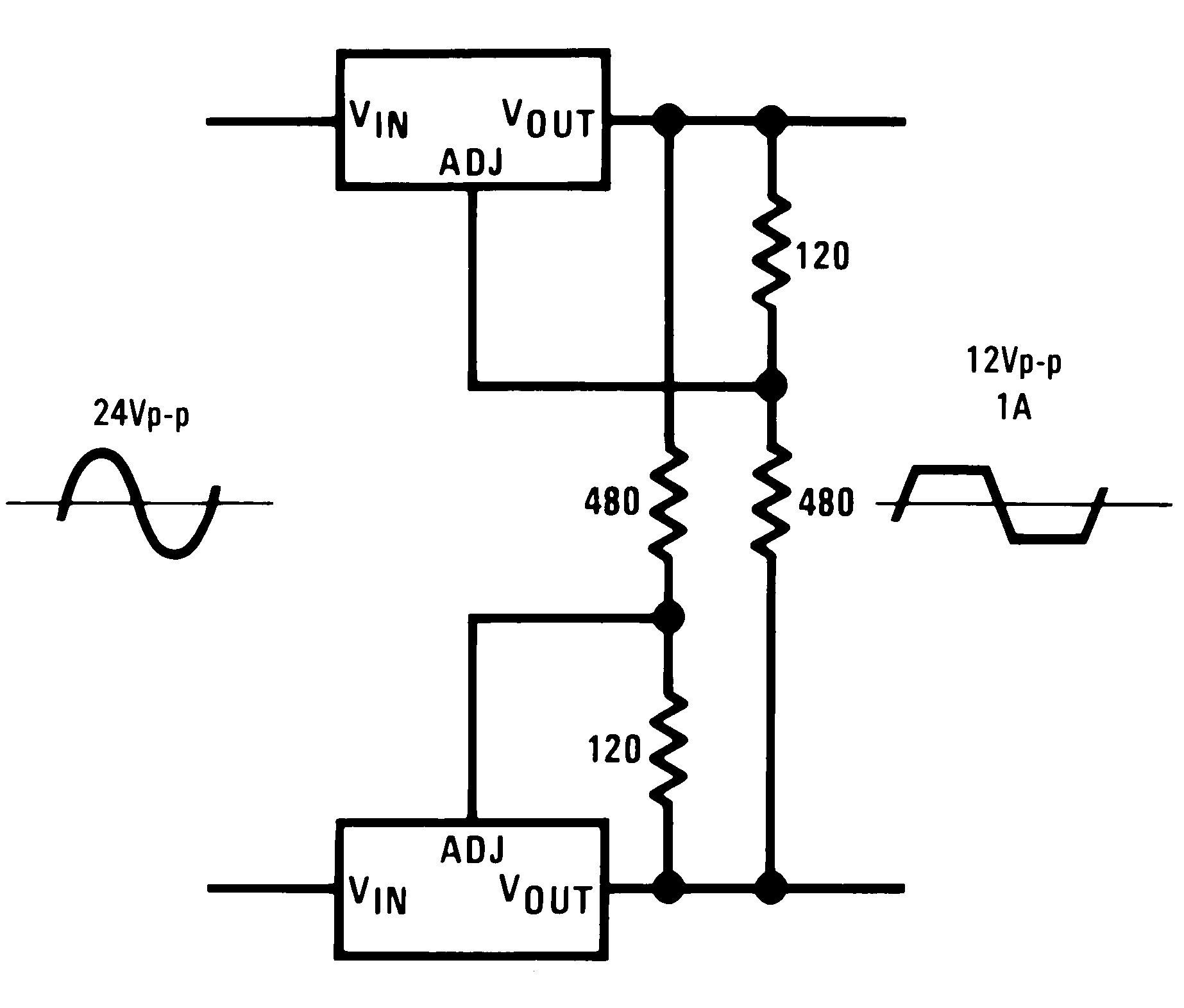 Figure 29. AC Voltage Regulator
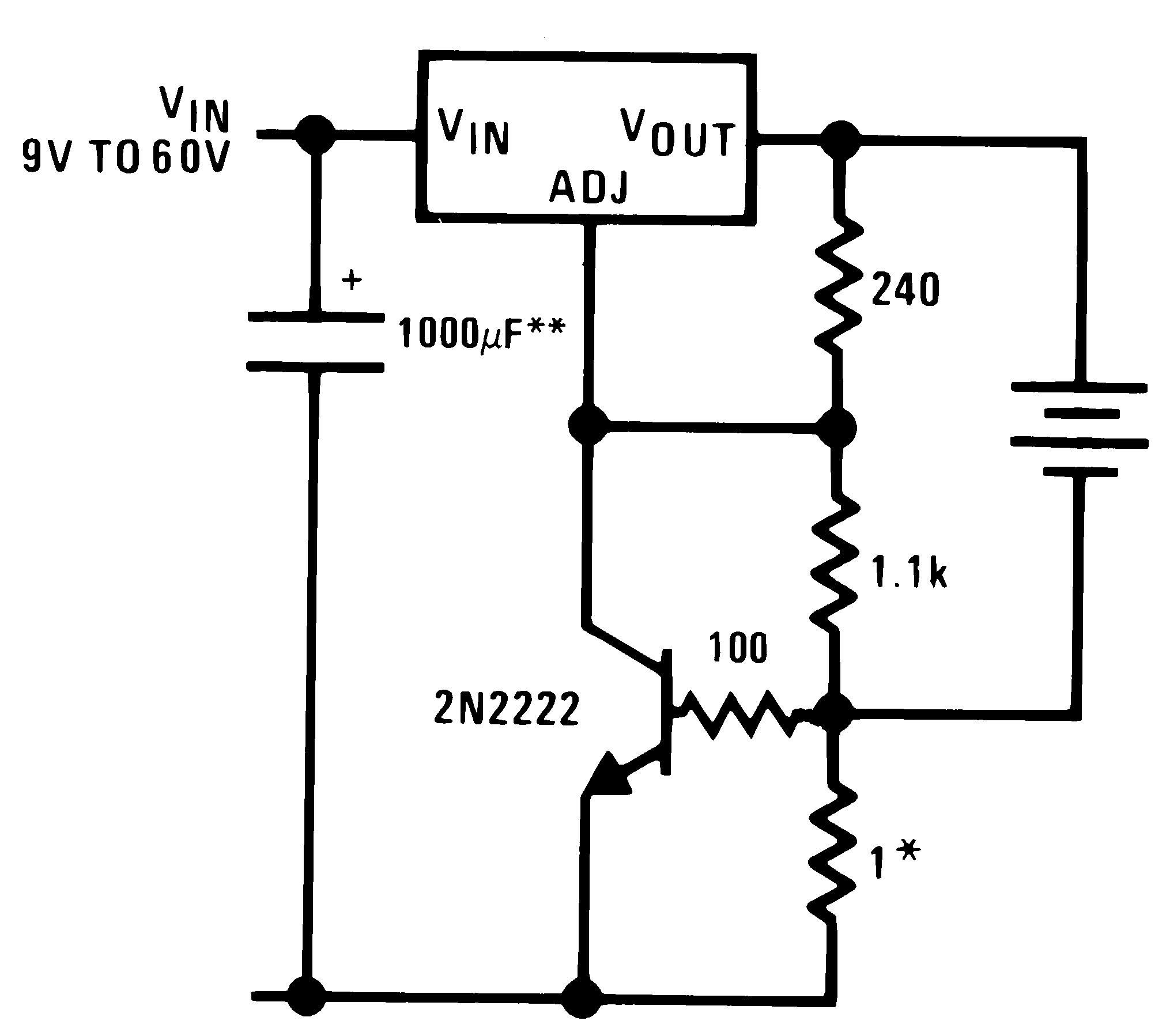
8.2.14 12-V Battery Charger
The LM317HV-MIL can be used in a battery charger application, where the device maintains either constant voltage or constant current mode depending on the current charge of the battery. To do this, the part senses the voltage drop across the battery and delivers the maximum charging current necessary to charge the battery. When the battery charge is low, there exists a voltage drop across the sense resistor RS, providing constant current to the battery at that instant. As the battery approaches full charge, the potential drop across RS approaches zero, reducing the current and maintaining the fixed voltage of the battery.
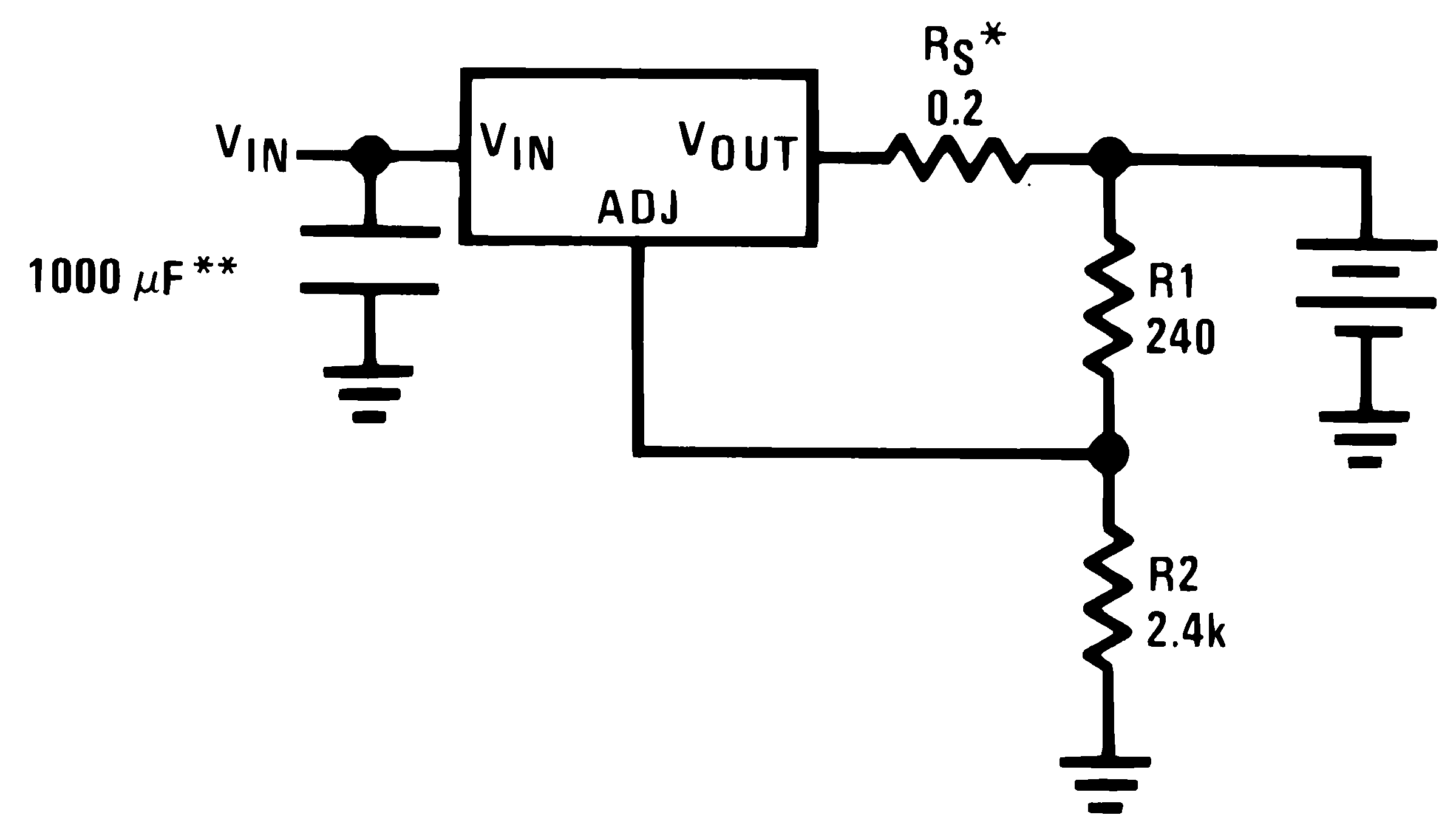

Use of RS allows low charging rates with fully charged battery.
**The 1000 μF is recommended to filter out input transients
8.2.15 Adjustable 4-A Regulator
Using three LM317HV-MIL devices in parallel increases load current capability. Output voltage is set by the variable resistor tied to the non-inverting terminal of the op amp, and reference current to the transistor is developed across the 100-Ω resistor. When output voltage rises, the op amp corrects by drawing current from the base, closing the transistor. This effectively pulls ADJ down and lowers the output voltage through negative feedback.
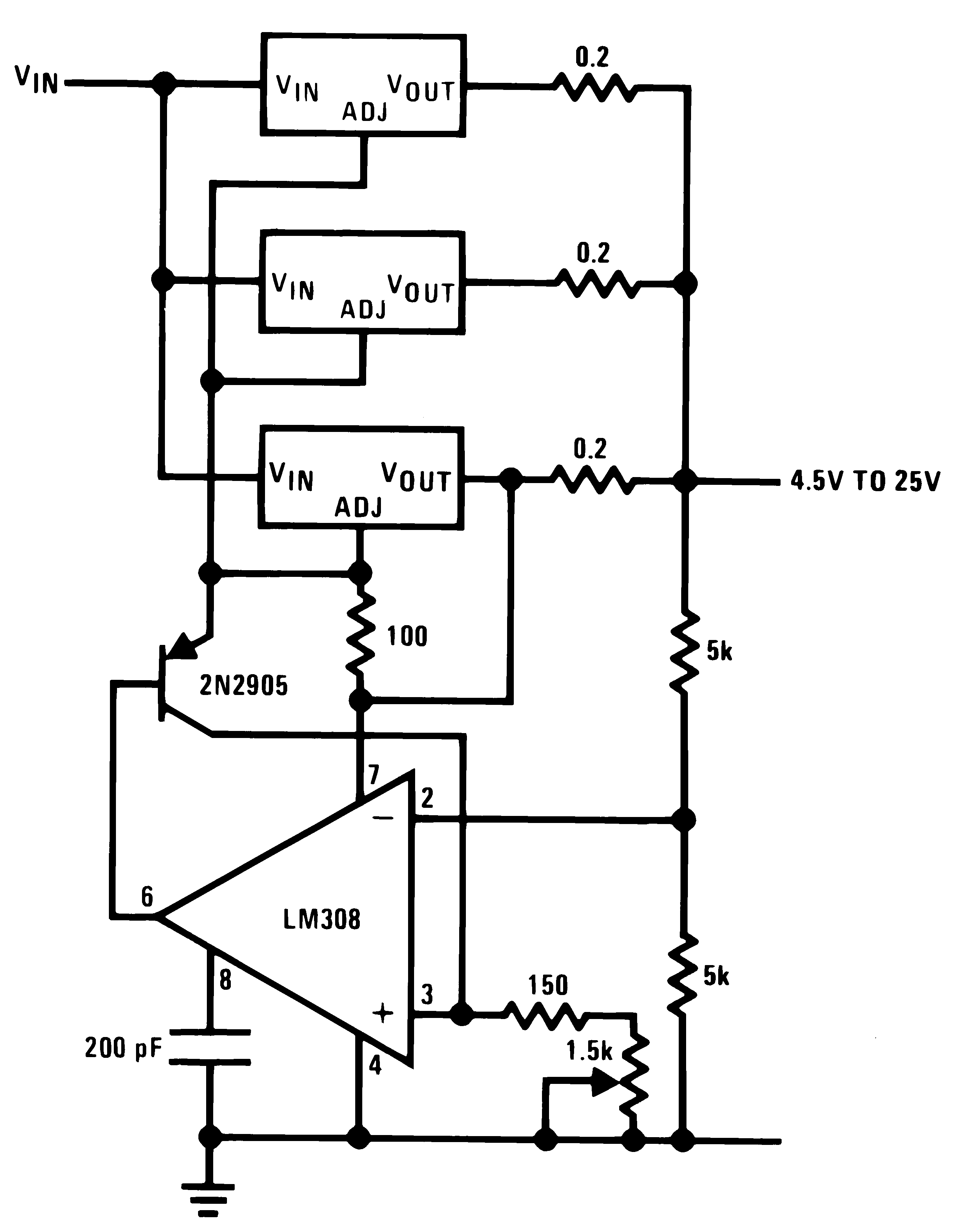 Figure 31. Adjustable 4-A Regulator
8.2.16 Current Limited 6-V Charger
The current in a battery charger application is limited by switching between constant current and constant voltage states. When the battery pulls low current, the drop across the 1-Ω resistor is not substantial and the NPN remains off. A constant voltage is seen across the battery, as regulated by the resistor divider. When current through the battery rises past peak current, the 1 Ω provides enough voltage to turn the transistor on, pulling ADJ close to ground. This results in limiting the maximum current to the battery.
