SNOSC16D March 2000 – January 2015 LM124-N , LM224-N , LM2902-N , LM324-N
PRODUCTION DATA.
1 Features
- Internally Frequency Compensated for Unity Gain
- Large DC Voltage Gain 100 dB
- Wide Bandwidth (Unity Gain) 1 MHz
(Temperature Compensated) - Wide Power Supply Range:
- Single Supply 3 V to 32 V
- or Dual Supplies ±1.5 V to ±16 V
- Very Low Supply Current Drain (700 μA)
—Essentially Independent of Supply Voltage - Low Input Biasing Current 45 nA
(Temperature Compensated) - Low Input Offset Voltage 2 mV
and Offset Current: 5 nA - Input Common-Mode Voltage Range Includes Ground
- Differential Input Voltage Range Equal to the Power Supply Voltage
- Large Output Voltage Swing 0 V to V+ − 1.5 V
-
Advantages:
- Eliminates Need for Dual Supplies
- Four Internally Compensated Op Amps in a Single Package
- Allows Direct Sensing Near GND and VOUT also Goes to GND
- Compatible With All Forms of Logic
- Power Drain Suitable for Battery Operation
- In the Linear Mode the Input Common-Mode, Voltage Range Includes Ground and the Output Voltage
- Can Swing to Ground, Even Though Operated from Only a Single Power Supply Voltage
- Unity Gain Cross Frequency is Temperature Compensated
- Input Bias Current is Also Temperature Compensated
2 Applications
- Transducer Amplifiers
- DC Gain Blocks
- Conventional Op Amp Circuits
3 Description
The LM124-N series consists of four independent, high-gain, internally frequency compensated operational amplifiers designed to operate from a single power supply over a wide range of voltages. Operation from split-power supplies is also possible and the low-power supply current drain is independent of the magnitude of the power supply voltage.
Application areas include transducer amplifiers, DC gain blocks and all the conventional op amp circuits which now can be more easily implemented in single power supply systems. For example, the LM124-N series can directly operate off of the standard 5-V power supply voltage which is used in digital systems and easily provides the required interface electronics without requiring the additional ±15 V power supplies.
Device Information(1)
| PART NUMBER | PACKAGE | BODY SIZE (NOM) |
|---|---|---|
| LM124-N | CDIP (14) | 19.56 mm × 6.67 mm |
| LM224-N | ||
| LM324-N | CDIP (14) | 19.56 mm × 6.67 mm |
| PDIP (14) | 19.177 mm × 6.35 mm | |
| SOIC (14) | 8.65 mm × 3.91 mm | |
| TSSOP (14) | 5.00 mm × 4.40 mm | |
| LM2902-N | PDIP (14) | 19.177 mm × 6.35 mm |
| SOIC (14) | 8.65 mm × 3.91 mm | |
| TSSOP (14) | 5.00 mm × 4.40 mm |
- For all available packages, see the orderable addendum at the end of the datasheet.
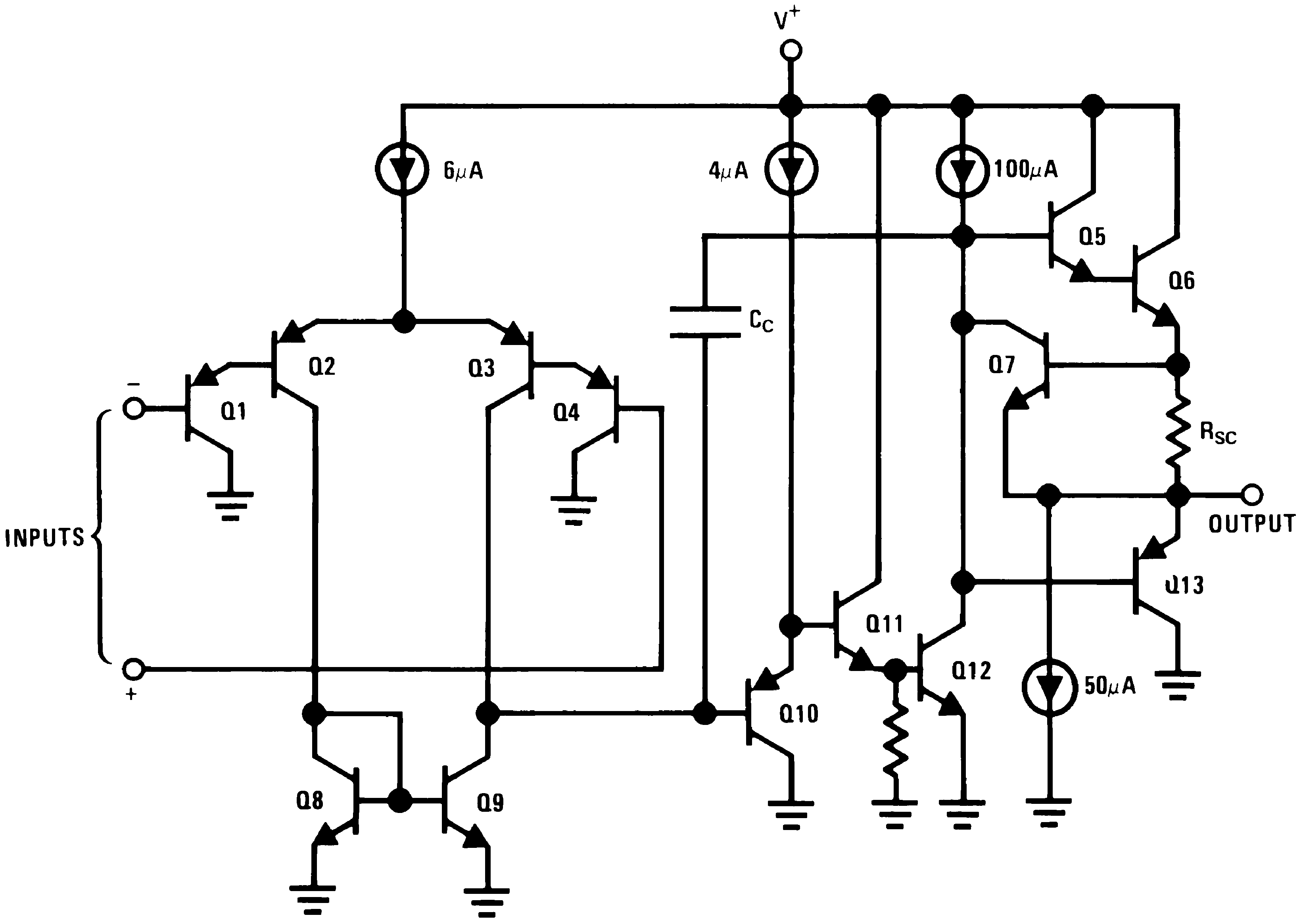
Schematic Diagram

4 Revision History
Changes from C Revision (November 2012) to D Revision
- Added Pin Configuration and Functions section, ESD Ratings table, Feature Description section, Device Functional Modes, Application and Implementation section, Power Supply Recommendations section, Layout section, Device and Documentation Support section, and Mechanical, Packaging, and Orderable Information sectionGo