SNOSB48E October 2011 – August 2015 LM3242
PRODUCTION DATA.
- 1 Features
- 2 Applications
- 3 Description
- 4 Revision History
- 5 Pin Configuration and Functions
- 6 Specifications
- 7 Detailed Description
- 8 Application and Implementation
- 9 Power Supply Recommendations
- 10Layout
- 11Device and Documentation Support
- 12Mechanical, Packaging, and Orderable Information
8 Application and Implementation
NOTE
Information in the following applications sections is not part of the TI component specification, and TI does not warrant its accuracy or completeness. TI’s customers are responsible for determining suitability of components for their purposes. Customers should validate and test their design implementation to confirm system functionality.
8.1 Application Information
8.1.1 Setting The Output Voltage
The LM3242 features a pin-controlled adjustable output voltage to eliminate the need for external feedback resistors. It can be programmed for an output voltage from 0.4 V to 3.6 V by setting the voltage on the VCON pin, as in Equation 1:
When VCON is between 0.16 V and 1.44 V, the output voltage will follow proportionally by 2.5 times of VCON.
If VCON is less than 0.16 V (VOUT = 0.4 V), the output voltage may not be well regulated. Refer to Figure 21 for more detail. This curve exhibits the characteristics of a typical part, and the performance cannot be ensured as there could be a part-to-part variation for output voltages less than 0.4 V. For VOUT lower than 0.4 V, the converter might suffer from larger output ripple voltage and higher current limit operation.
8.1.2 FB
Typically the FB pin is connected to VOUT for regulating the output voltage maximum of 3.6 V.
8.2 Typical Application
 Figure 23. LM3242 Typical Application
8.2.1 Design Requirements
For typical step-down DC-DC applications, use the parameters listed in Table 2.
Table 2. Design Parameters
| DESIGN PARAMETER | EXAMPLE VALUE |
|---|---|
| Minimum input voltage | 2.7 V |
| Minimum output voltage | 0.4 V |
| Output current | 0 to 750 mA |
| Switching frequency | 6 MHz (typical) |
8.2.2 Detailed Design Procedure
8.2.2.1 Inductor Selection
There are two main considerations when choosing an inductor; the inductor must not saturate, and the inductor current ripple is small enough to achieve the desired output voltage ripple. Different manufacturers follow different saturation current rating specifications, so attention must be given to details. Saturation current ratings are typically specified at 25°C so ratings over the ambient temperature of application should be requested from manufacturer.
Minimum value of inductance to ensure good performance is 0.3 µH at bias current (ILIM (typical)) over the ambient temperature range. Shielded inductors radiate less noise and are preferred. There are two methods to choose the inductor saturation current rating:
8.2.2.1.1 Method 1
The saturation current must be greater than the sum of the maximum load current and the worst-case average-to-peak inductor current. This can be written as:

where
- IRIPPLE: average-to-peak inductor current
- IOUT_MAX: maximum load current (750 mA)
- VIN: maximum input voltage in application
- L minimum inductor value including worst-case tolerances (30% drop can be considered for Method 1)
- F: minimum switching frequency (5.7 MHz)
- VOUT: output voltage
8.2.2.1.2 Method 2
A more conservative and recommended approach is to choose an inductor that can handle the maximum current limit of 1600 mA.
The resistance of the inductor must be less than approximately 0.1 Ω for good efficiency. Table 3 lists suggested inductors and suppliers.
Table 3. Suggested Inductors
| MODEL | SIZE (W × L × H) (mm) | VENDOR |
|---|---|---|
| MIPSZ2012D0R5 | 2 × 1.2 × 1 | FDK |
| LQM21PNR54MG0 | 2 × 1.25 × 0.9 | Murata |
| LQM2MPNR47NG0 | 2 × 1.6 × 0.9 | Murata |
| CIG21LR47M | 2 × 1.25 × 1 | Samsung |
| CKP2012NR47M | 2 × 1.25 × 1 | Taiyo Yuden |
8.2.2.2 Capacitor Selection
The LM3242 is designed for use with ceramic capacitors for its input and output filters. Use a 10-µF ceramic capacitor for input and a sum total of 4.7-µF ceramic capacitors for the output. They must maintain at least 50% capacitance at DC bias and temperature conditions. Ceramic capacitors types such as X5R, X7R, and B are recommended for both filters. These provide an optimal balance between small size, cost, reliability and performance for cell phones and similar applications. Table 4 lists some suggested part numbers and suppliers. DC bias characteristics of the capacitors must be considered when selecting the voltage rating and case size of the capacitor. If it is necessary to choose a 0603 (1608) size capacitor for VIN and 0402 (1005) size capacitor for VOUT, the operation of the LM3242 must be carefully evaluated on the system board. Use of a 2.2-µF capacitor in conjunction with multiple 0.47 µF or 1 µF capacitors in parallel may also be considered when connecting to power amplifier devices that require local decoupling.
Table 4. Suggested Capacitors and Their Suppliers
| CAPACITANCE | MODEL | SIZE (W × L) (mm) | VENDOR |
|---|---|---|---|
| 2.2 µF | GRM155R60J225M | 1 × 0.5 | Murata |
| 2.2 µF | C1005X5R0J225M | 1 × 0.5 | TDK |
| 2.2 µF | CL05A225MQ5NSNC | 1 × 0.5 | Samsung |
| 4.7 µF | C1608JB0J475M | 1.6 × 0.8 | TDK |
| 4.7 µF | C1005X5R0J475M | 1 × 0.5 | TDK |
| 4.7 µF | CL05A475MQ5NRNC | 1 × 0.5 | Samsung |
| 10 µF | C1608X5R0J106M | 1.6 × 0.8 | TDK |
| 10 µF | GRM155R60J106M | 1 × 0.5 | Murata |
| 10 µF | CL05A106MQ5NUNC | 1 × 0.5 | Samsung |
The input filter capacitor supplies AC current drawn by the PFET switch of the LM3242 in the first part of each cycle and reduces the voltage ripple imposed on the input power source. The output filter capacitor absorbs the AC inductor current, helps maintain a steady output voltage during transient load changes and reduces output voltage ripple. These capacitors must be selected with sufficient capacitance and sufficiently low Equivalent Series Resistance (ESR) to perform these functions. The ESR of the filter capacitors is generally a major factor in voltage ripple.
8.2.3 Application Curves
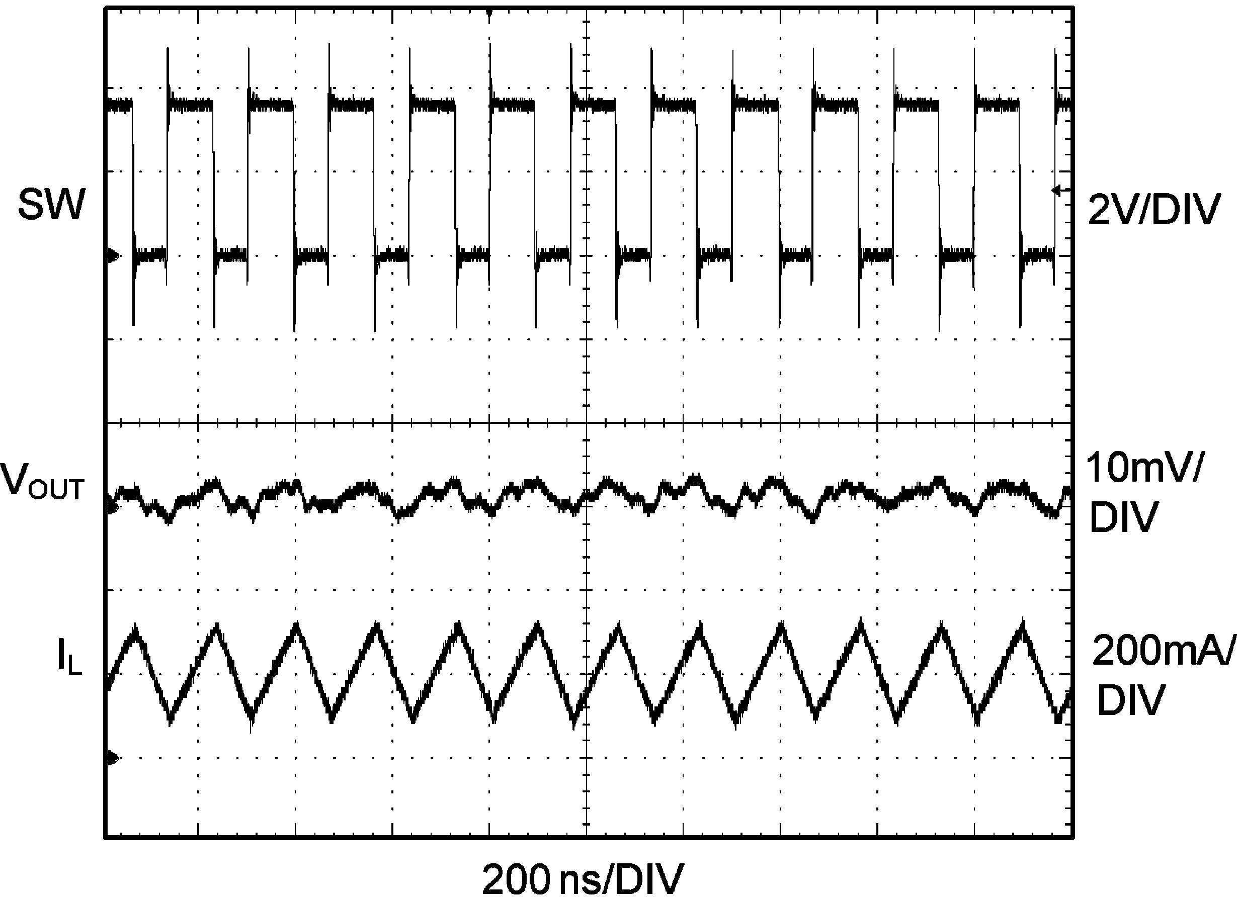
| VOUT = 2 V | IOUT = 200 mA | |
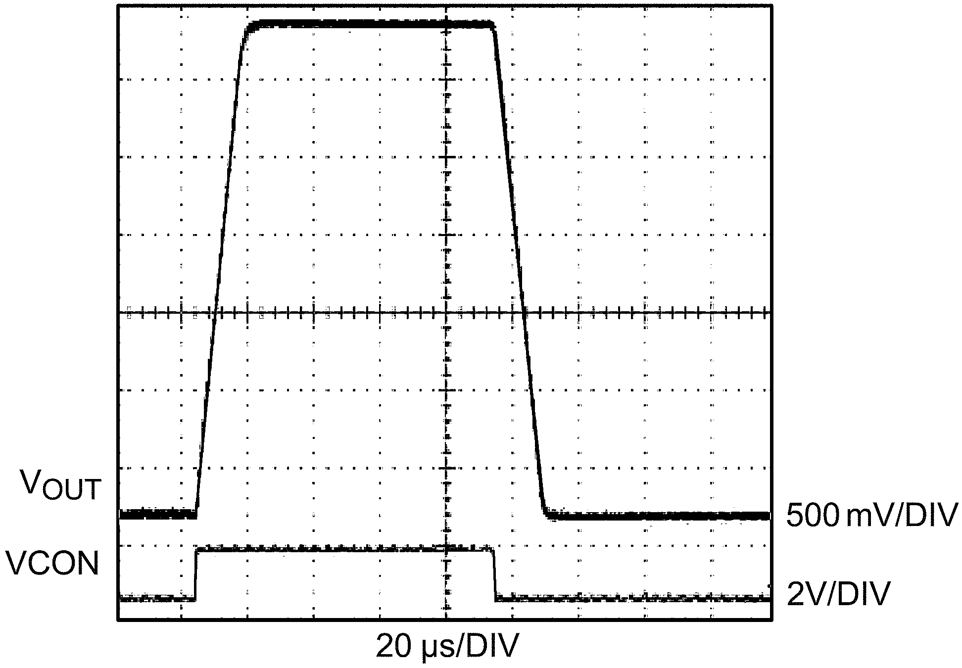
| VIN = 3.9 V | VOUT = 0.4 V to 3.6 V | RLOAD=10 Ω |
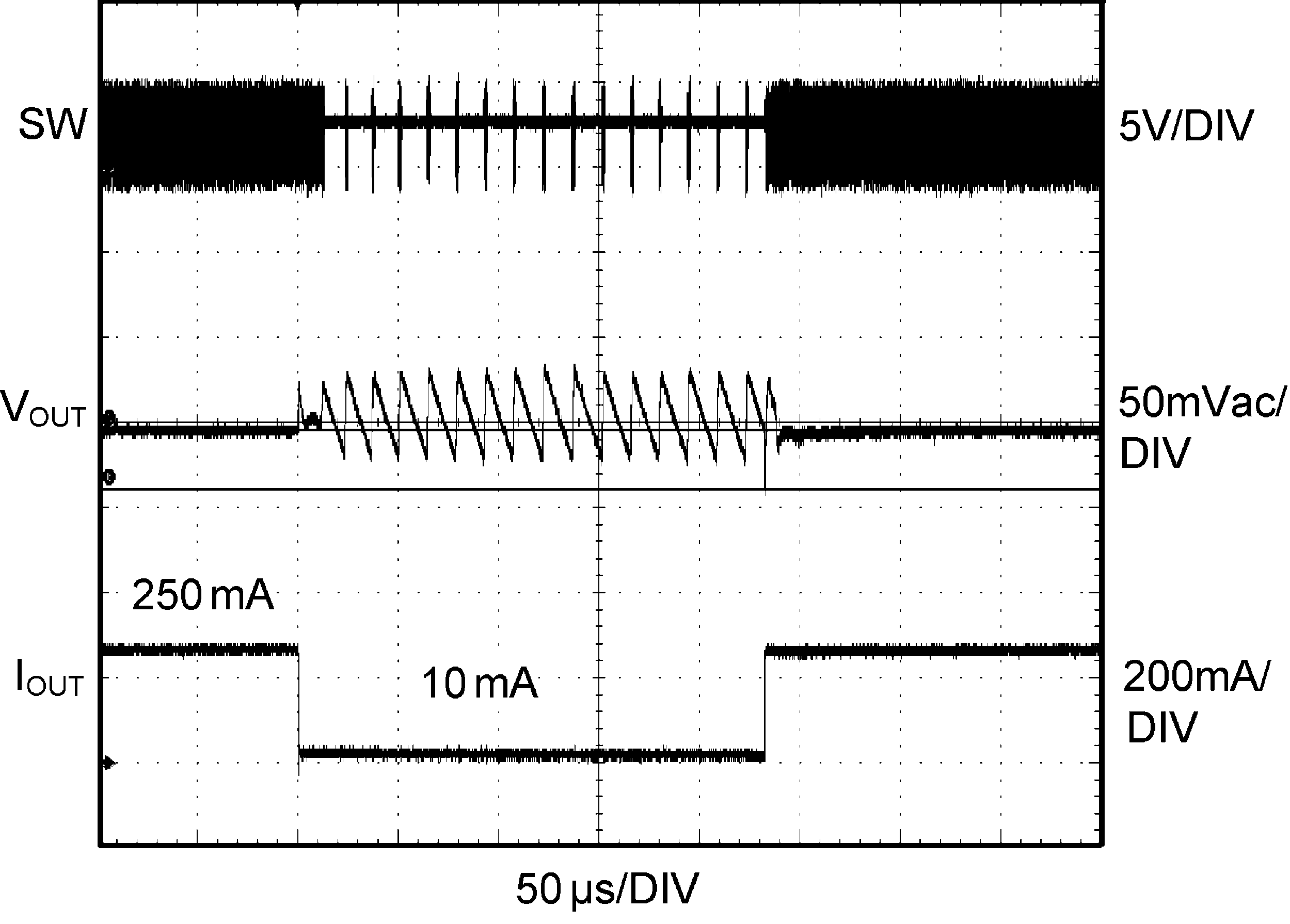
| VOUT = 2.5 V | IOUT = 10 mA/250 mA | |
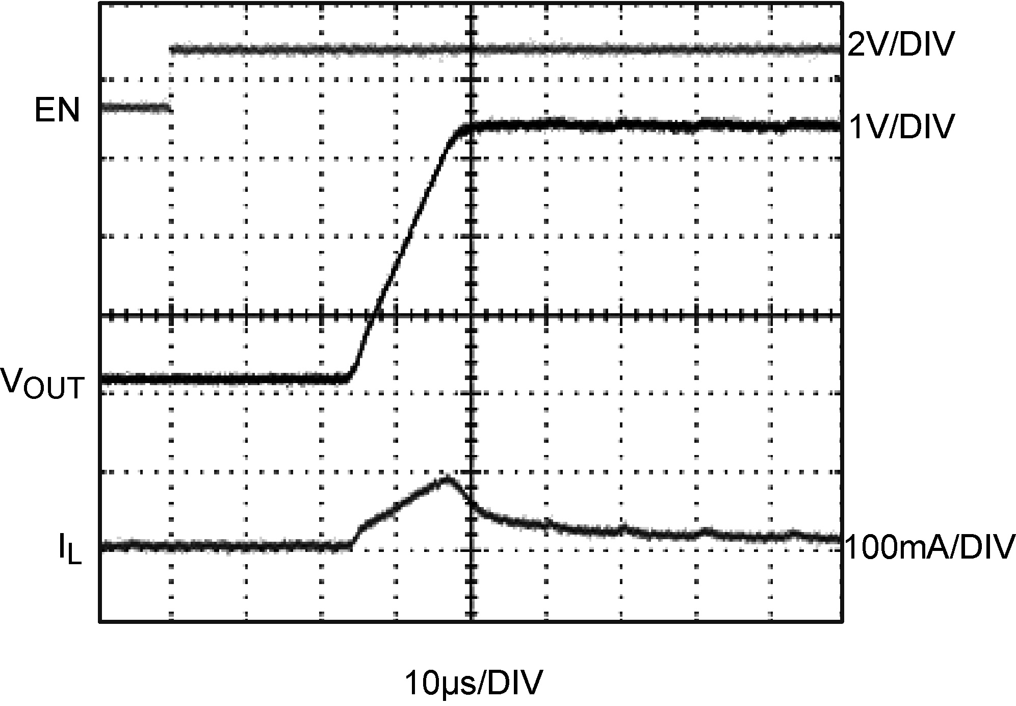
| VIN = 4.2 V | VOUT = 2.4 V | RLOAD= 3.6 Ω | ||
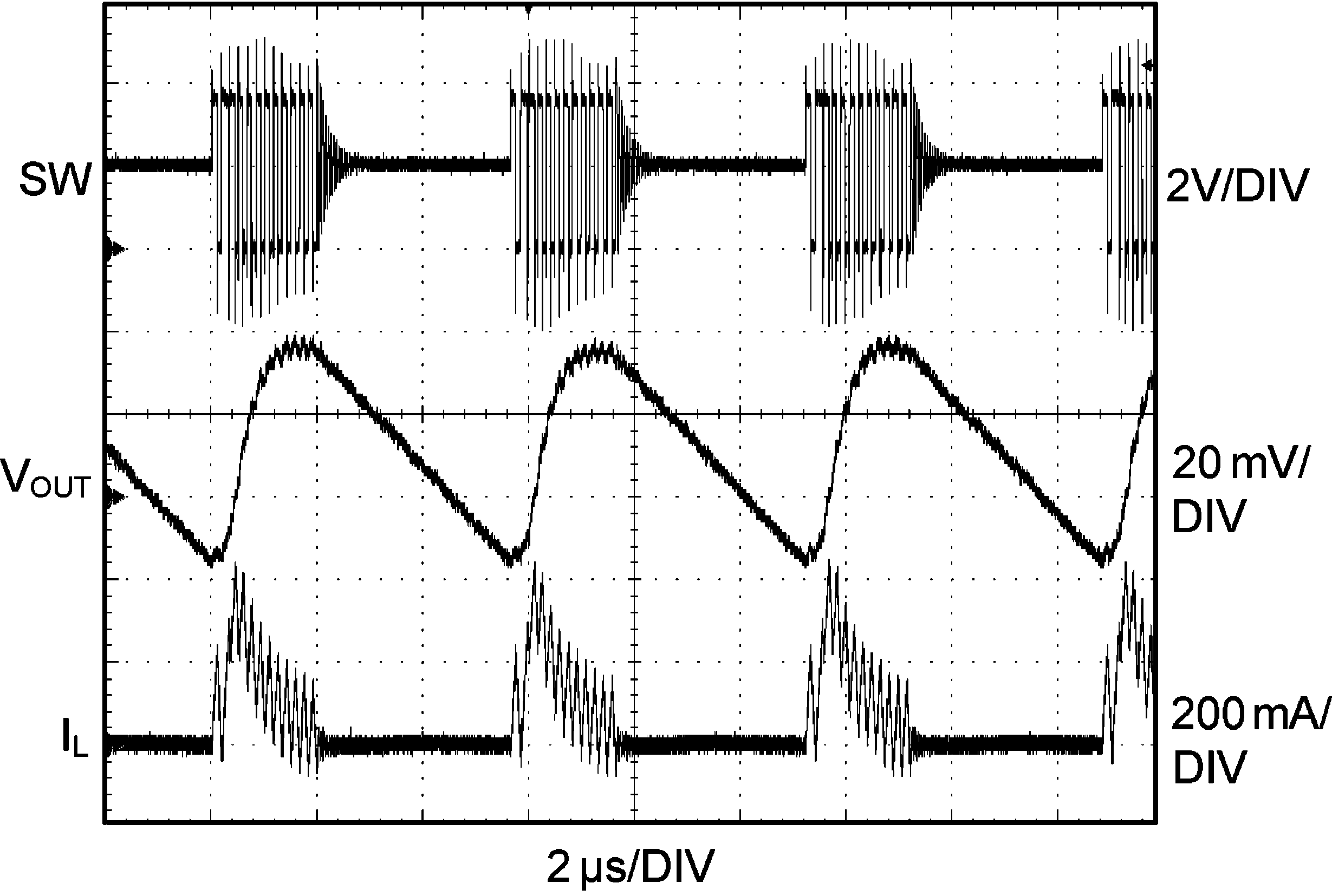
| VOUT = 2 V | IOUT = 50 mA | |
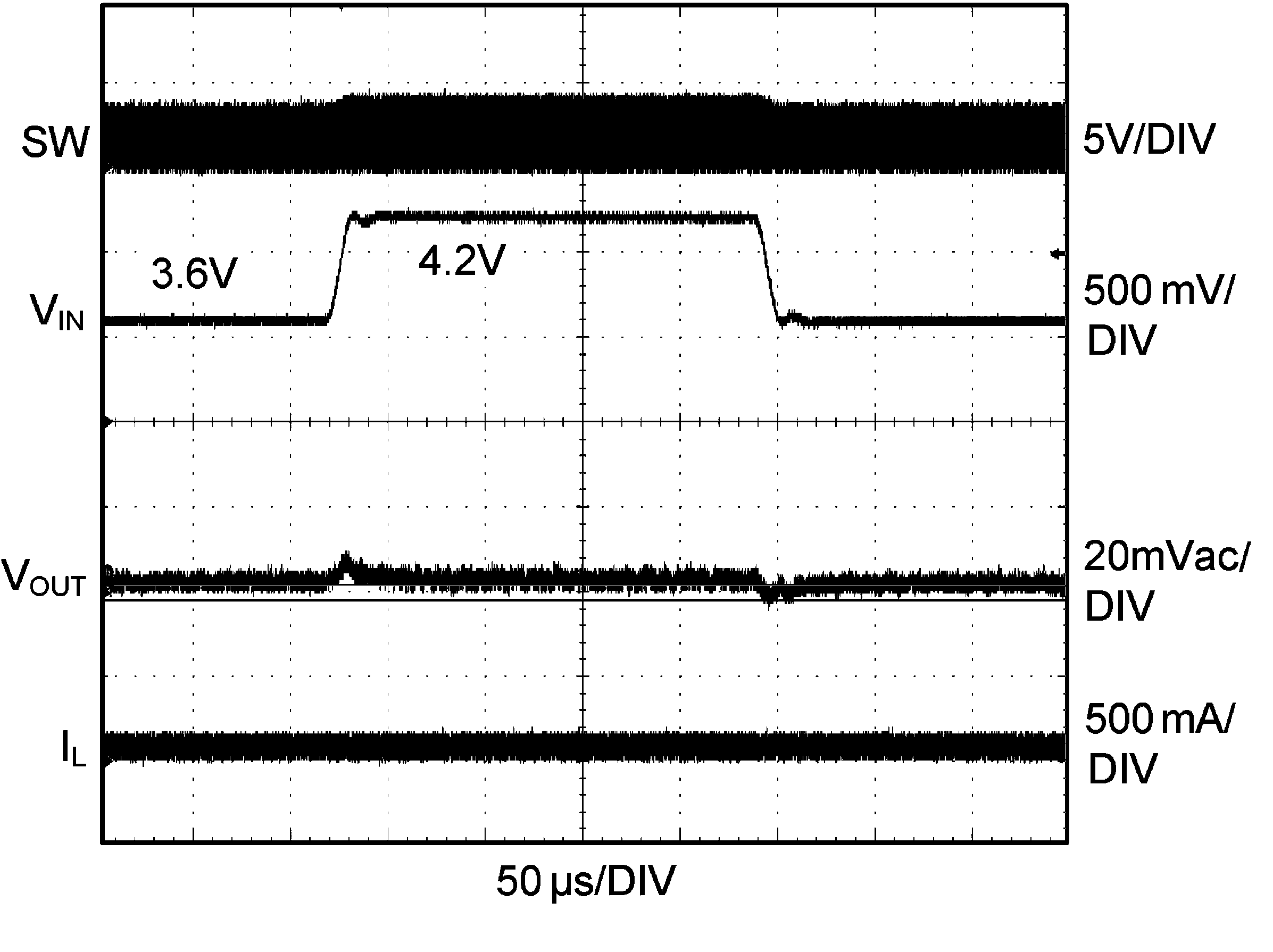
| VIN = 3.6 V to 4.2 V | VOUT = 0.8 V | RLOAD= 8 Ω |
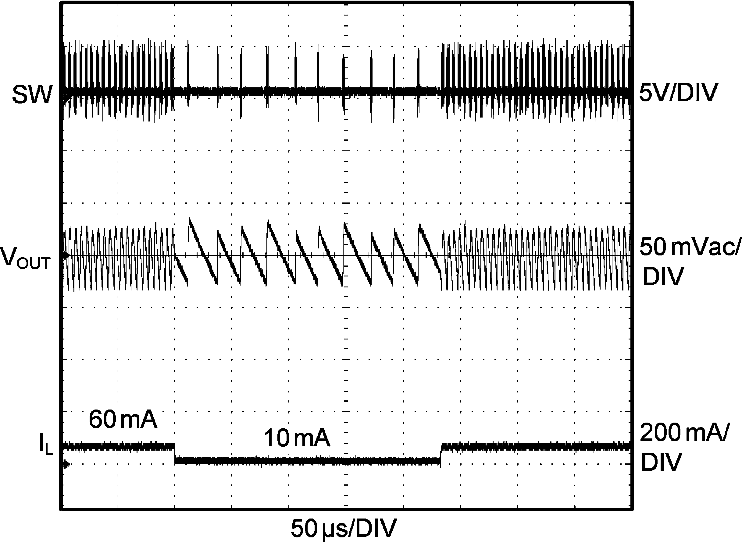
| VOUT = 0.6 V | IOUT = 10 mA/60 mA | |