JAJSDB1 June 2017 LM340-MIL
PRODUCTION DATA.
10 Layout
10.1 Layout Guidelines
Some layout guidelines must be followed to ensure proper regulation of the output voltage with minimum noise. Traces carrying the load current must be wide to reduce the amount of parasitic trace inductance. To improve PSRR, a bypass capacitor can be placed at the OUTPUT pin and must be placed as close as possible to the IC. All that is required for the typical fixed output regulator application circuit is the LM340-MIL IC and a 0.22-µF input capacitor if the regulator is placed far from the power supply filter. A 0.1-µF output capacitor is recommended to help with transient response. In cases when VIN shorts to ground, an external diode must be placed from VOUT to VIN to divert the surge current from the output capacitor and help protect the device.
10.2 Layout Example
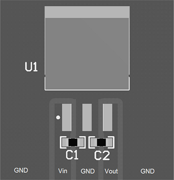 Figure 27. Layout Example DDPAK
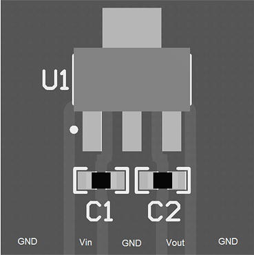 Figure 28. Layout Example SOT-223
10.3 Heat Sinking DDPAK/TO-263 and SOT-223 Package Parts
Both the DDPAK/TO-263 (KTT) and SOT-223 (DCY) packages use a copper plane on the PCB and the PCB itself as a heat sink. To optimize the heat sinking ability of the plane and PCB, solder the tab of the plane.
Figure 29 shows for the DDPAK/TO-263 the measured values of θ(J–A) for different copper area sizes using a typical PCB with 1-oz copper and no solder mask over the copper area used for heat sinking.
As shown in Figure 29, increasing the copper area beyond 1 square inch produces very little improvement. It should also be observed that the minimum value of θ(J–A) for the DDPAK/TO-263 package mounted to a PCB is 32°C/W.
As a design aid, Figure 30 shows the maximum allowable power dissipation compared to ambient temperature for the DDPAK/TO-263 device (assuming θ(J–A) is 35°C/W and the maximum junction temperature is 125°C).
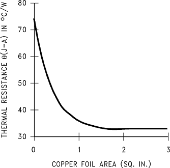 Figure 29. θ(J–A) vs Copper (1 Ounce) Area for the DDPAK/TO-263 Package
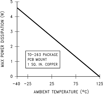 Figure 30. Maximum Power Dissipation vs TAMB for the DDPAK/TO-263 Package
Figure 31 and Figure 32 show the information for the SOT-223 package. Figure 31 assumes a θ(J–A) of 74°C/W for 1-oz. copper and 51°C/W for 2-oz. copper and a maximum junction temperature of 125°C.
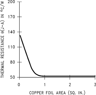 Figure 31. θ(J–A) vs Copper (2 Ounce) Area
for the SOT-223 Package
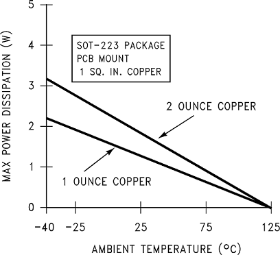 Figure 32. Maximum Power Dissipation vs
TAMB for the SOT-223 Package
See AN-1028 LMX2370 PLLatinum Dual Freq Synth for RF Pers Comm LMX2370 2.5GHz/1.2GHz for power enhancement techniques to be used with the SOT-223 package.