SNVS450F September 2006 – October 2015 LM3402 , LM3402HV
PRODUCTION DATA.
- 1 Features
- 2 Applications
- 3 Description
- 4 Revision History
- 5 Pin Configuration and Functions
- 6 Specifications
- 7 Detailed Description
-
8 Application and Implementation
- 8.1 Application Information
- 8.2 Typical Application
- 9 Power Supply Recommendations
- 10Layout
- 11Device and Documentation Support
- 12Mechanical, Packaging, and Orderable Information
7 Detailed Description
7.1 Overview
The LM3402 and LM3402HV are buck regulators with a wide input voltage range, low voltage reference, and a fast output enable/disable function. These features combine to make them ideal for use as a constant current source for LEDs with forward currents as high as 500 mA. The controlled ON-time (COT) architecture is a combination of hysteretic mode control and a one-shot ON-timer that varies inversely with input voltage. Hysteretic operation eliminates the need for small-signal control loop compensation. When the converter runs in continuous conduction mode (CCM) the controlled ON-time maintains a constant switching frequency over the range of input voltage. Fast transient response, PWM dimming, a low power shutdown mode, and simple output overvoltage protection round out the functions of the LM3402/HV.
7.2 Functional Block Diagram

7.3 Feature Description
7.3.1 Controlled ON-time Overview
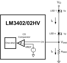
Figure 17 shows the feedback system used to control the current through an array of LEDs. A voltage signal, VSNS, is created as the LED current flows through the current setting resistor, RSNS, to ground. VSNS is fed back to the CS pin, where it is compared against a 200-mV reference, VREF. The ON-comparator turns on the power MOSFET when VSNS falls below VREF. The power MOSFET conducts for a controlled ON-time, tON, set by an external resistor, RON, and by the input voltage, VIN. ON-time is governed using Equation 1.

At the conclusion of tON the power MOSFET turns off for a minimum OFF-time, tOFF-MIN, of 300 ns. Once tOFF-MIN is complete the CS comparator compares VSNS and VREF again, waiting to begin the next cycle.
 Figure 17. Comparator and One-Shot
The LM3402/HV regulators should be operated in continuous conduction mode (CCM), where inductor current stays positive throughout the switching cycle. During steady-state operation in the CCM, the converter maintains a constant switching frequency, which can be selected using Equation 2.

7.3.2 Average LED Current Accuracy
The COT architecture regulates the valley of ΔVSNS, the AC portion of VSNS. To determine the average LED current (which is also the average inductor current) the valley inductor current is calculated using Equation 4.

In Equation 4 tSNS represents the propagation delay of the CS comparator, and is approximately 220 ns. The average inductor/LED current is equal to IL-MIN plus one-half of the inductor current ripple, ΔiL:
Detailed information for the calculation of ΔiL is given in the Application and Implementation section.
7.3.3 Maximum Output Voltage
The 300 ns minimum off-time limits on the maximum duty cycle of the converter, DMAX, and in turn ,the maximum output voltage VO(MAX) is determined by Equation 6:

The maximum number of LEDs, nMAX, that can be placed in a single series string is governed by VO(MAX) and the maximum forward voltage of the LEDs used, VF(MAX), using the expression:

At low switching frequency the maximum duty cycle and output voltage are higher, allowing the LM3402/HV to regulate output voltages that are nearly equal to input voltage. The following equation relates switching frequency to maximum output voltage.

7.3.4 Minimum Output Voltage
The minimum recommended ON-time for the LM3402/HV is 300 ns. This lower limit for tON determines the minimum duty cycle and output voltage that can be regulated based on input voltage and switching frequency. The relationship is determined by the following equation:

7.3.5 High Voltage Bias Regulator
The LM3402/HV contains an internal linear regulator with a 7-V output, connected between the VIN and the VCC pins. The VCC pin should be bypassed to the GND pin with a 0.1-µF ceramic capacitor connected as close as possible to the pins of the device. VCC tracks VIN until VIN reaches 8.8 V (typical) and then regulates at 7 V as VIN increases. Operation begins when VCC crosses 5.25 V.
7.3.6 Internal MOSFET and Driver
The LM3402/HV features an internal power MOSFET as well as a floating driver connected from the SW pin to the BOOT pin. Both rise time and fall time are 20 ns each (typical) and the approximate gate charge is 3 nC. The high-side rail for the driver circuitry uses a bootstrap circuit consisting of an internal high-voltage diode and an external 10 nF capacitor, CB. VCC charges CB through the internal diode while the power MOSFET is off. When the MOSFET turns on, the internal diode reverse biases. This creates a floating supply equal to the VCC voltage minus the diode drop to drive the MOSFET when its source voltage is equal to VIN.
7.3.7 Fast Shutdown for PWM Dimming
The DIM pin of the LM3402/HV is a TTL logic compatible input for low-frequency PWM dimming of the LED. A logic low (less than 0.8V) at DIM will disable the internal MOSFET and shut off the current flow to the LED array. While the DIM pin is in a logic low state the support circuitry (driver, bandgap, VCC) remains active to minimize the time needed to turn the LED array back on when the DIM pin sees a logic high (above 2.2 V). A 75 µA (typical) pullup current ensures that the LM3402/HV is on when DIM pin is open circuited, eliminating the need for a pullup resistor. Dimming frequency, fDIM, and duty cycle, DDIM, are limited by the LED current rise time and fall time and the delay from activation of the DIM pin to the response of the internal power MOSFET. In general, fDIM should be at least one order of magnitude lower than the steady state switching frequency to prevent aliasing.
7.3.8 Peak Current Limit
The current limit comparator of the LM3402/HV will engage whenever the power MOSFET current (equal to the inductor current while the MOSFET is on) exceeds 735 mA (typical). The power MOSFET is disabled for a cool-down time that is 10x the steady-state ON-time. At the conclusion of this cool-down time the system re-starts. If the current limit condition persists the cycle of cool-down time and restarting will continue, creating a low-power hiccup mode, minimizing thermal stress on the LM3402/HV and the external circuit components.
7.3.9 Overvoltage and Overcurrent Comparator
The CS pin includes an output overvoltage/overcurrent comparator that will disable the power MOSFET whenever VSNS exceeds 300 mV. This threshold provides a hard limit for the output current. Output current overshoot is limited to 300 mV / RSNS by this comparator during transients.
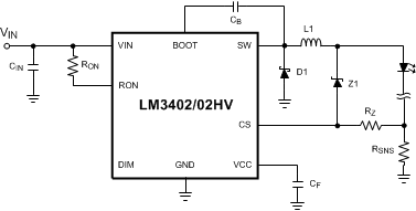
The OVP/OCP comparator can also be used to prevent the output voltage from rising to VO(MAX) in the event of an output open-circuit. This is the most common failure mode for LEDs, due to breaking of the bond wires. In a current regulator an output open circuit causes VSNS to fall to zero, commanding maximum duty cycle. Figure 18 shows a method using a Zener diode, Z1, and Zener limiting resistor, RZ, to limit output voltage to the reverse breakdown voltage of Z1 plus 200 mV. The Zener diode reverse breakdown voltage, VZ, must be greater than the maximum combined VF of all LEDs in the array. The maximum recommended value for RZ is 1 kΩ.
As discussed in the Maximum Output Voltage section, there is a limit to how high VO can rise during an output open-circuit that is always less than VIN. If no output capacitor is used, the output stage of the LM3402/HV is capable of withstanding VO(MAX) indefinitely, however the voltage at the output end of the inductor will oscillate and can go above VIN or less than 0 V. A small (typically 10 nF) capacitor across the LED array dampens this oscillation. For circuits that use an output capacitor, the system can still withstand VO(MAX) indefinitely as long as CO is rated to handle VIN. The high current paths are blocked in output open-circuit and the risk of thermal stress is minimal, hence the user may opt to allow the output voltage to rise in the case of an open-circuit LED failure.
 Figure 18. Output Open Circuit Protection
7.4 Device Functional Modes
7.4.1 Low Power Shutdown
The LM3402/HV can be switched to a low power state (IIN-SD = 90 µA) by grounding the RON pin with a signal-level MOSFET as shown in Figure 19. Low power MOSFETs like the 2N7000, 2N3904, or equivalent are recommended devices for putting the LM3402/HV into low power shutdown. Logic gates can also be used to shut down the LM3402/HV as long as the logic low voltage is below the over temperature minimum threshold of 0.3V. Noise filter circuitry on the RON pin can cause a few pulses with a longer ON-time than normal after RON is grounded or released. In these cases the OVP/OCP comparator will ensure that the peak inductor or LED current does not exceed 300 mV / RSNS.
 Figure 19. Low Power Shutdown
7.4.2 Thermal Shutdown
Internal thermal shutdown circuitry is provided to protect the device in the event that the maximum junction temperature is exceeded. The threshold for thermal shutdown is 165°C with a 25°C hysteresis (both values typical). During thermal shutdown the MOSFET and driver are disabled.