SNVS602L March 2009 – June 2016 LM3409 , LM3409-Q1 , LM3409HV , LM3409HV-Q1
PRODUCTION DATA.
- 1 Features
- 2 Applications
- 3 Description
- 4 Revision History
- 5 Device Comparison Table
- 6 Pin Configuration and Functions
- 7 Specifications
-
8 Detailed Description
- 8.1 Overview
- 8.2 Functional Block Diagram
- 8.3 Feature Description
- 8.4 Device Functional Modes
-
9 Application and Implementation
- 9.1
Application Information
- 9.1.1 Input Undervoltage Lockout (UVLO)
- 9.1.2 Operation Near Dropout
- 9.1.3 LED Ripple Current
- 9.1.4 Buck Converters without Output Capacitors
- 9.1.5 Buck Converters With Output Capacitors
- 9.1.6 Output Overvoltage Protection
- 9.1.7 Input Capacitors
- 9.1.8 P-Channel MOSFET (PFET)
- 9.1.9 Re-Circulating Diode
- 9.2
Typical Applications
- 9.2.1 EN PIN PWM Dimming Application for 10 LEDs
- 9.2.2 Analog Dimming Application for 4 LEDs
- 9.2.3 LM3409 Buck Converter Application
- 9.1
Application Information
- 10Power Supply Recommendations
- 11Layout
- 12Device and Documentation Support
- 13Mechanical, Packaging, and Orderable Information
パッケージ・オプション
メカニカル・データ(パッケージ|ピン)
- DGQ|10
サーマルパッド・メカニカル・データ
- DGQ|10
発注情報
1 Features
- LM3409-Q1 and LM3409HV-Q1 are Automotive Grade Products: AEC-Q100 Grade 1 Qualified
- 2-Ω, 1-A Peak MOSFET Gate Drive
- VIN Range: 6 V to 42 V (LM3409, LM3409-Q1)
- VIN Range: 6 V to 75 V (LM3409HV, LM3409HV-Q1)
- Differential, High-Side Current Sense
- Cycle-by-Cycle Current Limit
- No Control Loop Compensation Required
- 10,000:1 PWM Dimming Range
- 250:1 Analog Dimming Range
- Supports All-Ceramic Output Capacitors and Capacitor-less Outputs
- Low-Power Shutdown and Thermal Shutdown
- Thermally Enhanced 10-Pin, HVSSOP Package
2 Applications
- LED Driver
- Constant Current Source
- Automotive Lighting
- General Illumination
3 Description
The LM3409, LM3409-Q1, LM3409HV, and LM3409HV-Q1 are P-channel MOSFET (PFET) controllers for step-down (buck) current regulators. They offer wide input voltage range, high-side differential current sense with low adjustable threshold voltage and fast output enable/disable function and a thermally enhanced 10-pin, HVSSOP package. These features combine to make the LM3409 family of devices ideal for use as constant current sources for driving LEDs where forward currents up to 5 A are easily achievable.
The LM3409 devices use constant off-time (COFT) control to regulate an accurate constant current without the need for external control loop compensation. Analog and PWM dimming are easy to implement and result in a highly linear dimming range with excellent achievable contrast ratios. Programmable UVLO, low-power shutdown, and thermal shutdown complete the feature set.
Device Information(1)
| PART NUMBER | PACKAGE | BODY SIZE (NOM) |
|---|---|---|
| LM3409 | HVSSOP (10) | 3.00 mm × 3.00 mm |
| PDIP (14) | 19.177 mm × 6.35 mm | |
| LM3409-Q1 | HVSSOP (10) | 3.00 mm × 3.00 mm |
| LM3409HV | ||
| LM3409HV-Q1 |
- For all available packages, see the orderable addendum at the end of the data sheet.
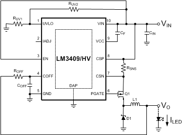
Typical Application Schematic
