SNVS602L March 2009 – June 2016 LM3409 , LM3409-Q1 , LM3409HV , LM3409HV-Q1
PRODUCTION DATA.
- 1 Features
- 2 Applications
- 3 Description
- 4 Revision History
- 5 Device Comparison Table
- 6 Pin Configuration and Functions
- 7 Specifications
-
8 Detailed Description
- 8.1 Overview
- 8.2 Functional Block Diagram
- 8.3 Feature Description
- 8.4 Device Functional Modes
-
9 Application and Implementation
- 9.1
Application Information
- 9.1.1 Input Undervoltage Lockout (UVLO)
- 9.1.2 Operation Near Dropout
- 9.1.3 LED Ripple Current
- 9.1.4 Buck Converters without Output Capacitors
- 9.1.5 Buck Converters With Output Capacitors
- 9.1.6 Output Overvoltage Protection
- 9.1.7 Input Capacitors
- 9.1.8 P-Channel MOSFET (PFET)
- 9.1.9 Re-Circulating Diode
- 9.2
Typical Applications
- 9.2.1 EN PIN PWM Dimming Application for 10 LEDs
- 9.2.2 Analog Dimming Application for 4 LEDs
- 9.2.3 LM3409 Buck Converter Application
- 9.1
Application Information
- 10Power Supply Recommendations
- 11Layout
- 12Device and Documentation Support
- 13Mechanical, Packaging, and Orderable Information
8 Detailed Description
8.1 Overview
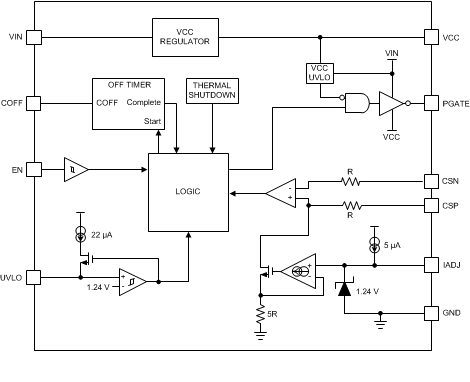
The LM3409/09HV are P-channel MOSFET (PFET) controllers for step-down (buck) current regulators which are ideal for driving LED loads. They have wide input voltage range allowing for regulation of a variety of LED loads. The high-side differential current sense, with low adjustable threshold voltage, provides an excellent method for regulating output current while maintaining high system efficiency.
The LM3409/09HV uses a Controlled Off-Time (COFT) architecture that allows the converter to be operated in both continuous conduction mode (CCM) and discontinuous conduction mode (DCM) with no external control loop compensation, while providing an inherent cycle-by-cycle current limit. The adjustable current sense threshold provides the capability to amplitude (analog) dim the LED current over the full range and the fast output enable/disable function allows for high frequency PWM dimming using no external components.
When designing, the maximum attainable LED current is not internally limited because the LM3409/09HV is a controller. Instead it is a function of the system operating point, component choices, and switching frequency allowing the LM3409/09HV to easily provide constant currents up to 5A. This simple controller contains all the features necessary to implement a high-efficiency versatile LED driver.
8.2 Functional Block Diagram
8.3 Feature Description
8.3.1 Buck Current Regulators
The buck regulator is unique among non-isolated topologies due to the direct connection of the inductor to the load during the entire switching cycle. An inductor will control the rate of change of current that flows through it, therefore a direct connection to the load is excellent for current regulation. A buck current regulator, using the LM3409/09HV, is shown in the Application and Implementation section. During the time that the PFET (Q1) is turned on (tON), the input voltage charges up the inductor (L1). When Q1 is turned off (tOFF), the re-circulating diode (D1) becomes forward biased and L1 discharges. During both intervals, the current is supplied to the load keeping the LEDs forward biased. Figure 19 shows the inductor current (iL(t)) waveform for a buck converter operating in CCM.
The average inductor current (IL) is equal to the average output LED current (ILED), therefore if IL is tightly controlled, ILED will be well regulated. As the system changes input voltage or output voltage, duty cycle (D) is varied to regulate IL and ultimately ILED. For any buck regulator, D is simply the conversion ratio divided by the efficiency (η):

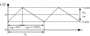 Figure 19. Ideal CCM Buck Converter Inductor Current iL(t)
8.3.2 Controlled Off-Time (COFT) Architecture
The COFT architecture is used by the LM3409/09HV to control ILED. It is a combination of peak current detection and a one-shot off-timer that varies with output voltage. D is indirectly controlled by changes in both tOFF and tON, which vary depending on the operating point. This creates a variable switching frequency over the entire operating range. This type of hysteretic control eliminates the need for control loop compensation necessary in many switching regulators, simplifying the design process and providing fast transient response.
8.3.2.1 Adjustable Peak Current Control
At the beginning of a switching period, PFET Q1 is turned on and inductor current increases. Once peak current is detected, Q1 is turned off, the diode D1 forward biases, and inductor current decreases. Figure 20 shows how peak current detection is accomplished using the differential voltage signal created as current flows through the current setting resistor (RSNS). The voltage across RSNS (VSNS) is compared to the adjustable current sense threshold (VCST) and Q1 is turned off when VSNS exceeds VCST, providing that tON is greater than the minimum possible tON (typically 115ns).
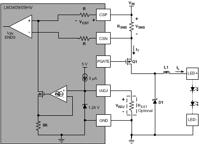 Figure 20. Peak Current Control Circuit
There are three different methods to set the current sense threshold (VCST) using the multi-function IADJ pin:
- IADJ pin left open: 5 µA internal current source biases the Zener diode and clamps the IADJ pin voltage (VADJ) at 1.24 V causing the maximum threshold voltage:
- External voltage (VADJ) of 0 V to 1.24 V: Apply to the IADJ pin to adjust VCST from 0V to 248mV. If the VADJ voltage is adjustable, analog dimming can be achieved.
- External resistor (REXT) placed from IADJ pin to ground: 5 µA current source sets the VADJ voltage and corresponding threshold voltage:


8.3.2.2 Controlled Off-Time
Once Q1 is turned off, it remains off for a constant time (tOFF) which is preset by an external resistor (ROFF), an external capacitor (COFF), and the output voltage (VO) as shown in Figure 21. Because ILED is tightly regulated, VO will remain nearly constant over widely varying input voltage and temperature yielding a nearly constant tOFF.
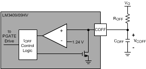 Figure 21. Off-Time Control Circuit
At the start of tOFF, the voltage across COFF (vCOFF(t)) is zero and the capacitor begins charging according to the time constant provided by ROFF and COFF. When vCOFF(t) reaches the off-time threshold (VOFT = 1.24 V), then the off-time is terminated and vCOFF(t) is reset to zero. tOFF is calculated as follows:

In reality, there is typically 20 pF parasitic capacitance at the off-timer pin in parallel with COFF, which is accounted for in the calculation of tOFF. Also, it should be noted that the tOFF equation has a preceding negative sign because the result of the logarithm should be negative for a properly designed circuit. The resulting tOFF is a positive value as long as VO > 1.24 V. If VO < 1.24 V, the off-timer cannot reach VOFT and an internally limited maximum off-time (typically 300 µs) will occur.
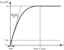 Figure 22. Exponential Charging Function vCOFF(t)
Although the tOFF equation is non-linear, tOFF is actually very linear in most applications. Ignoring the 20-pF parasitic capacitance at the COFF pin, vCOFF(t) is plotted in Figure 22. The time derivative of vCOFF(t) can be calculated to find a linear approximation to the tOFF equation:

When tOFF << ROFF x COFF (equivalent to when VO >> 1.24V), the slope of the function is essentially linear and tOFF can be approximated as a current source charging COFF:

Using the actual tOFF equation, the inductor current ripple (ΔiL-PP) of a buck current regulator operating in CCM is:

Using the tOFF approximation, the equation is reduced to:

NOTE
ΔiL-PP is independent of both VIN and VO when in CCM.
The ΔiL-PP approximation only depends on ROFF, COFF, and L1, therefore the ripple is essentially constant over the operating range as long as VO >> 1.24V (when the tOFF approximation is valid). An exception to the tOFF approximation occurs if the IADJ pin is used to analog dim. As the LED/inductor current decreases, the converter will eventually enter DCM and the ripple will decrease with the peak current threshold. The approximation shows how the LM3409/09HV achieves constant ripple over a wide operating range, however tOFF should be calculated using the actual equation first presented.
8.3.3 Average LED Current
For a buck converter, the average LED current is simply the average inductor current.
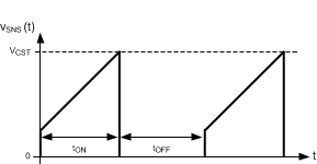 Figure 23. Sense Voltage vSNS(t)
Using the COFT architecture, the peak transistor current (IT-MAX) is sensed as shown in Figure 23, which is equal to the peak inductor current (IL-MAX) given by the following equation:

Because IL-MAX is set using peak current control and ΔiL-PP is set using the controlled off-timer, IL and correspondingly ILED can be calculated as follows:

The threshold voltage VCST seen by the high-side sense comparator is affected by the comparator’s input offset voltage, which causes an error in the calculation of IL-MAX and ultimately ILED. To mitigate this problem, the polarity of the comparator inputs is swapped every cycle, which causes the actual IL-MAX to alternate between two peak values (IL-MAXH and IL-MAXL), equidistant from the theoretical IL-MAX as shown in Figure 24. ILED remains accurate through this averaging.
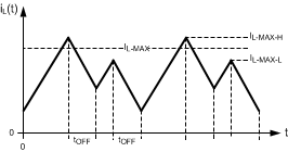 Figure 24. Inductor Current iL(t) Showing IL-MAX Offset
8.3.4 Inductor Current Ripple
Because the LM3409/09HV swaps the polarity of the differential current sense comparator every cycle, a minimum inductor current ripple (ΔiL-PP) is necessary to maintain accurate ILED regulation. Referring to Figure 24, the first tON is terminated at the higher of the two polarity-swapped thresholds (corresponding to IL-MAXH). During the following tOFF, iL decreases until the second tON begins. If tOFF is too short, then as the second tON begins, iL will still be above the lower peak current threshold (corresponding to IL-MAXL) and a minimum tON pulse will follow. This will result in degraded ILED regulation. The minimum inductor current ripple (ΔiL-PP-MIN) should adhere to the following equation to ensure accurate ILED regulation:

8.3.5 Switching Frequency
The switching frequency is dependent upon the actual operating point (VIN and VO). VO will remain relatively constant for a given application, therefore the switching frequency will vary with VIN (frequency increases as VIN increases). The target switching frequency (fSW) at the nominal operating point is selected based on the tradeoffs between efficiency (better at low frequency) and solution size/cost (smaller at high frequency). The off-time of the LM3409/09HV can be programmed for switching frequencies up to 5 MHz (theoretical limit imposed by minimum tON). In practice, switching frequencies higher than 1MHz may be difficult to obtain due to gate drive limitations, high input voltage, and thermal considerations.
At CCM operating points, fSW is defined as:

At DCM operating points, fSW is defined as:

In the CCM equation, it is apparent that the efficiency (η) factors into the switching frequency calculation. Efficiency is hard to estimate and, because switching frequency varies with input voltage, accuracy in setting the nominal switching frequency is not critical. Therefore, a general rule of thumb for the LM3409/09HV is to assume an efficiency between 85% and 100%. When approximating efficiency to target a nominal switching frequency, the following condition must be met:

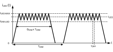 Figure 25. LED Current iLED(t) During EN Pin PWM Dimming
8.3.6 PWM Dimming Using the EN Pin
The enable pin (EN) is a TTL compatible input for PWM dimming of the LED. A logic low (below 0.5V) at EN will disable the internal driver and shut off the current flow to the LED array. While the EN pin is in a logic low state the support circuitry (driver, bandgap, VCC regulator) remains active to minimize the time needed to turn the LED array back on when the EN pin sees a logic high (above 1.74 V).
Figure 25 shows the LED current (iLED(t)) during PWM dimming where duty cycle (DDIM) is the percentage of the dimming period (TDIM) that the PFET is switching. For the remainder of TDIM, the PFET is disabled. The resulting dimmed average LED current (IDIM-LED) is:

The LED current rise and fall times (which are limited by the slew rate of the inductor as well as the delay from activation of the EN pin to the response of the external PFET) limit the achievable TDIM and DDIM. In general, dimming frequency should be at least one order of magnitude lower than the steady state switching frequency to prevent aliasing. However, for good linear response across the entire dimming range, the dimming frequency may need to be even lower.
8.3.7 High Voltage Negative BIAS Regulator
The LM3409/09HV contains an internal linear regulator where the steady state VCC pin voltage is typically 6.2 V below the voltage at the VIN pin. The VCC pin should be bypassed to the VIN pin with at least 1µF of ceramic capacitance connected as close as possible to the IC.
8.3.8 External Parallel FET PWM Dimming
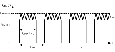 Figure 26. Ideal LED Current iLED(t) During Parallel FET Dimming
Any buck topology LED driver is a good candidate for parallel FET dimming because high slew rates are achievable, due to the fact that no output capacitance is required. This allows for much higher dimming frequencies than are achievable using the EN pin. When using external parallel FET dimming, a situation can arise where maximum off-time occurs due to a shorted output. To mitigate this situation, a secondary voltage (VDD) should be used as shown in Figure 27.
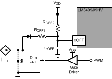 Figure 27. External Parallel FET Dimming Circuit
A small diode is connected in series with the off time resistor calculated for nominal operation from the output, ROFF1. Then connect a small diode from the secondary voltage along with another resistor, ROFF2. The secondary voltage can be any voltage as long as it is greater than 2V. The value of ROFF2 can be calculated using Equation 16.

The ideal LED current waveform iLED(t) during parallel FET PWM dimming is very similar to the EN pin PWM dimming shown previously. The LED current does not rise and fall infinitely fast as shown in Figure 26 however with this method, only the speed of the parallel Dim FET ultimately limits the dimming frequency and dimming duty cycle. This allows for much faster PWM dimming than can be attained with the EN pin.
8.4 Device Functional Modes
8.4.1 Low-Power Shutdown
The LM3409/09HV can be placed into a low-power shutdown (typically 110 µA) by grounding the EN terminal (any voltage below 0.5 V) until VCC drops below the VCC UVLO threshold (typically 3.73 V). During normal operation this terminal should be tied to a voltage above 1.74 V and below absolute maximum input voltage rating.
8.4.2 Thermal Shutdown
Internal thermal shutdown circuitry is provided to protect the IC in the event that the maximum junction temperature is exceeded. The threshold for thermal shutdown is 160°C with 15°C of hysteresis (both values typical). During thermal shutdown the PFET and driver are disabled.