JAJSAX0H October 2007 – August 2016 LM3410 , LM3410-Q1
PRODUCTION DATA.
- 1 特長
- 2 アプリケーション
- 3 概要
- 4 改訂履歴
- 5 Pin Configuration and Functions
- 6 Specifications
- 7 Detailed Description
-
8 Application and Implementation
- 8.1 Application Information
- 8.2
Typical Applications
- 8.2.1 Low Input Voltage, 1.6-MHz, 3 to 5 White LED Output at 50-mA Boost Converter
- 8.2.2 LM3410X SOT-23: 5 × 1206 Series LED String Application
- 8.2.3 LM3410Y SOT-23: 5 × 1206 Series LED String Application
- 8.2.4 LM3410X WSON: 7 × 5 LED Strings Backlighting Application
- 8.2.5 LM3410X WSON: 3 × HB LED String Application
- 8.2.6 LM3410Y SOT-23: 5 × 1206 Series LED String Application With OVP
- 8.2.7 LM3410X SEPIC WSON: HB or OLED Illumination Application
- 8.2.8 LM3410X WSON: Boost Flash Application
- 8.2.9 LM3410X SOT-23: 5 × 1206 Series LED String Application With VIN > 5.5 V
- 8.2.10 LM3410X WSON: Camera Flash or Strobe Circuit Application
- 8.2.11 LM3410X SOT-23: 5 × 1206 Series LED String Application With VIN and VPWR Rail > 5.5 V
- 8.2.12 LM3410X WSON: Boot-Strap Circuit to Extend Battery Life
- 9 Power Supply Recommendations
- 10Layout
- 11デバイスおよびドキュメントのサポート
- 12メカニカル、パッケージ、および注文情報
パッケージ・オプション
メカニカル・データ(パッケージ|ピン)
サーマルパッド・メカニカル・データ
- DGN|8
発注情報
6 Specifications
6.1 Absolute Maximum Ratings
over operating free-air temperature range (unless otherwise noted)(1)(2)| MIN | MAX | UNIT | ||
|---|---|---|---|---|
| Input voltage | VIN | –0.5 | 7 | V |
| SW | –0.5 | 26.5 | ||
| FB | –0.5 | 3 | ||
| DIM | –0.5 | 7 | ||
| Operating juction temperature(3), TJ | 150 | °C | ||
| Storage temperature, Tstg | –65 | 150 | °C | |
(1) Stresses beyond those listed under Absolute Maximum Ratings may cause permanent damage to the device. These are stress ratings only, which do not imply functional operation of the device at these or any other conditions beyond those indicated under Recommended Operating Conditions. Exposure to absolute-maximum-rated conditions for extended periods may affect device reliability.
(2) If Military/Aerospace specified devices are required, please contact the Texas Instruments Sales Office/Distributors for availability and specifications.
(3) Thermal shutdown occurs if the junction temperature exceeds the maximum junction temperature of the device.
6.2 ESD Ratings
| VALUE | UNIT | |||
|---|---|---|---|---|
| V(ESD) | Electrostatic discharge | Human-body model (HBM), per ANSI/ESDA/JEDEC JS-001(1) | ±2000 | V |
| Charged-device model (CDM), per JEDEC specification JESD22-C101(2) | ±1000 | |||
(1) JEDEC document JEP155 states that 500-V HBM allows safe manufacturing with a standard ESD control process.
(2) JEDEC document JEP157 states that 250-V CDM allows safe manufacturing with a standard ESD control process.
6.3 Recommended Operating Conditions
over operating free-air temperature range (unless otherwise noted)| MIN | MAX | UNIT | |||
|---|---|---|---|---|---|
| VIN | Input voltage | 2.7 | 5.5 | V | |
| VDIM | DIM control input(1) | 0 | VIN | V | |
| VSW | Switch output | 3 | 24 | V | |
| TJ | Operating junction temperature | –40 | 125 | °C | |
| Power dissipation (Internal) | SOT-23 | 400 | mW | ||
(1) Do not allow this pin to float or be greater than VIN + 0.3 V.
6.4 Thermal Information
| THERMAL METRIC(1) | LM3410, LM3410-Q1 | UNIT | ||||
|---|---|---|---|---|---|---|
| NGG (WSON) |
DGN (MSOP-PowerPAD) | DBV (SOT-23) |
||||
| 6 PINS | 8 PINS | 5 PINS | ||||
| RθJA | Junction-to-ambient thermal resistance | 0 LFPM Air Flow | 55.3 | 53.7 | 164.2 | °C/W |
| RθJC(top) | Junction-to-case (top) thermal resistance | 65.9 | 61.4 | 115.3 | °C/W | |
| RθJB | Junction-to-board thermal resistance | 29.6 | 37.3 | 27 | °C/W | |
| ψJT | Junction-to-top characterization parameter | 1.1 | 7.1 | 12.8 | °C/W | |
| ψJB | Junction-to-board characterization parameter | 29.7 | 37 | 26.5 | °C/W | |
| RθJC(bot) | Junction-to-case (bottom) thermal resistance | 9.3 | 6.8 | — | °C/W | |
(1) For more information about traditional and new thermal metrics, see the Semiconductor and IC Package Thermal Metrics application report.
6.5 Electrical Characteristics
Typical values apply for TJ = 25°C; Minimum and maximum limits apply for TJ = –40°C to 125°C and VIN = 5 V (unless otherwise noted). Typical values represent the most likely parametric norm at TJ = 25°C, and are provided for reference purposes only.| PARAMETER | TEST CONDITIONS | MIN | TYP | MAX | UNIT | |
|---|---|---|---|---|---|---|
| VFB | Feedback voltage | 178 | 190 | 202 | mV | |
| ΔVFB/VIN | Feedback voltage line regulation | VIN = 2.7 V to 5.5 V | 0.06 | %/V | ||
| IFB | Feedback input bias current | 0.1 | 1 | µA | ||
| fSW | Switching frequency | LM3410X | 1200 | 1600 | 2000 | kHz |
| LM3410Y | 360 | 525 | 680 | |||
| DMAX | Maximum duty cycle | LM3410X | 88% | 92% | ||
| LM3410Y | 90% | 95% | ||||
| DMIN | Minimum duty cycle | LM3410X | 5% | |||
| LM3410Y | 2% | |||||
| RDS(ON) | Switch on resistance | MSOP and SOT-23 | 170 | 330 | mΩ | |
| WSON | 190 | 350 | ||||
| ICL | Switch current limit | 2.1 | 2.8 | A | ||
| SU | Start-up time | 20 | µs | |||
| IQ | Quiescent current (switching) | LM3410X, VFB = 0.25 V | 7 | 11 | mA | |
| LM3410Y, VFB = 0.25 V | 3.4 | 7 | ||||
| Quiescent current (shutdown) | All versions, VDIM = 0 V | 80 | nA | |||
| UVLO | Undervoltage lockout | VIN rising | 2.3 | 2.65 | V | |
| VIN falling | 1.7 | 1.9 | ||||
| VDIM_H | Shutdown threshold voltage | 0.4 | V | |||
| Enable threshold voltage | 1.8 | |||||
| ISW | Switch leakage | VSW = 24 V | 1 | µA | ||
| IDIM | Dimming pin current | Sink and source | 100 | nA | ||
| TSD | Thermal shutdown temperature (1) | 165 | °C | |||
(1) Thermal shutdown occurs if the junction temperature exceeds the maximum junction temperature of the device.
6.6 Typical Characteristics
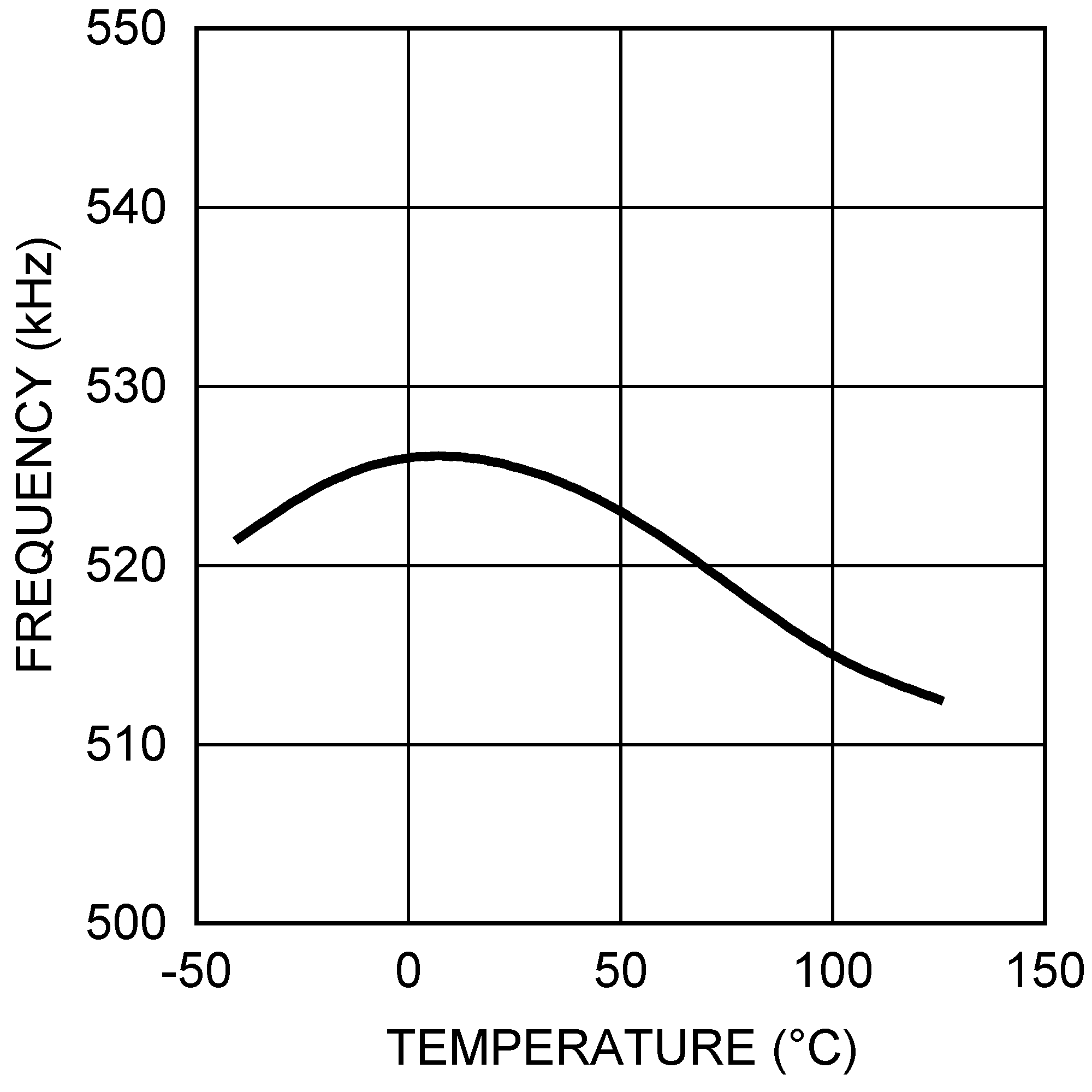
All curves taken at VIN = 5 V with the 50-mA boost configuration shown in Figure 18. TJ = 25°C, unless otherwise specified.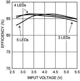
| RSET = 4 Ω |
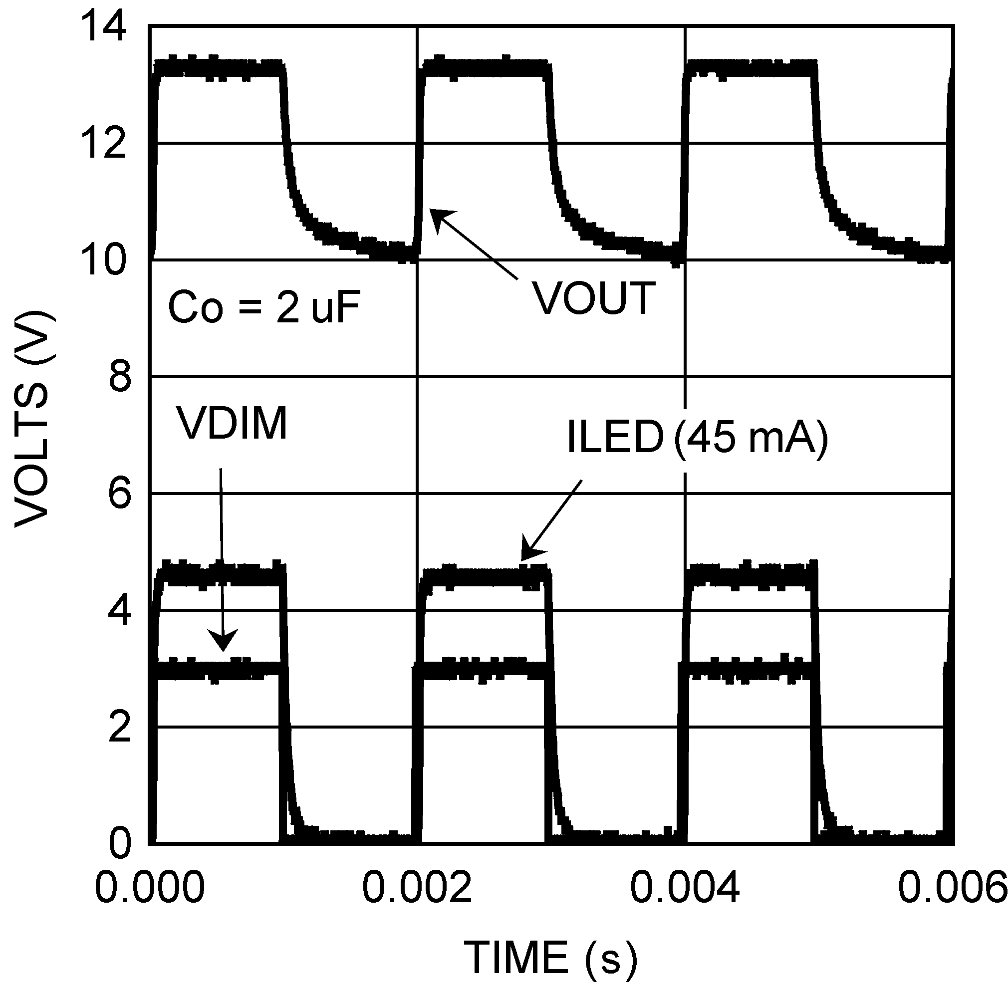
| 500-Hz DIM Frequency | D = 50% |
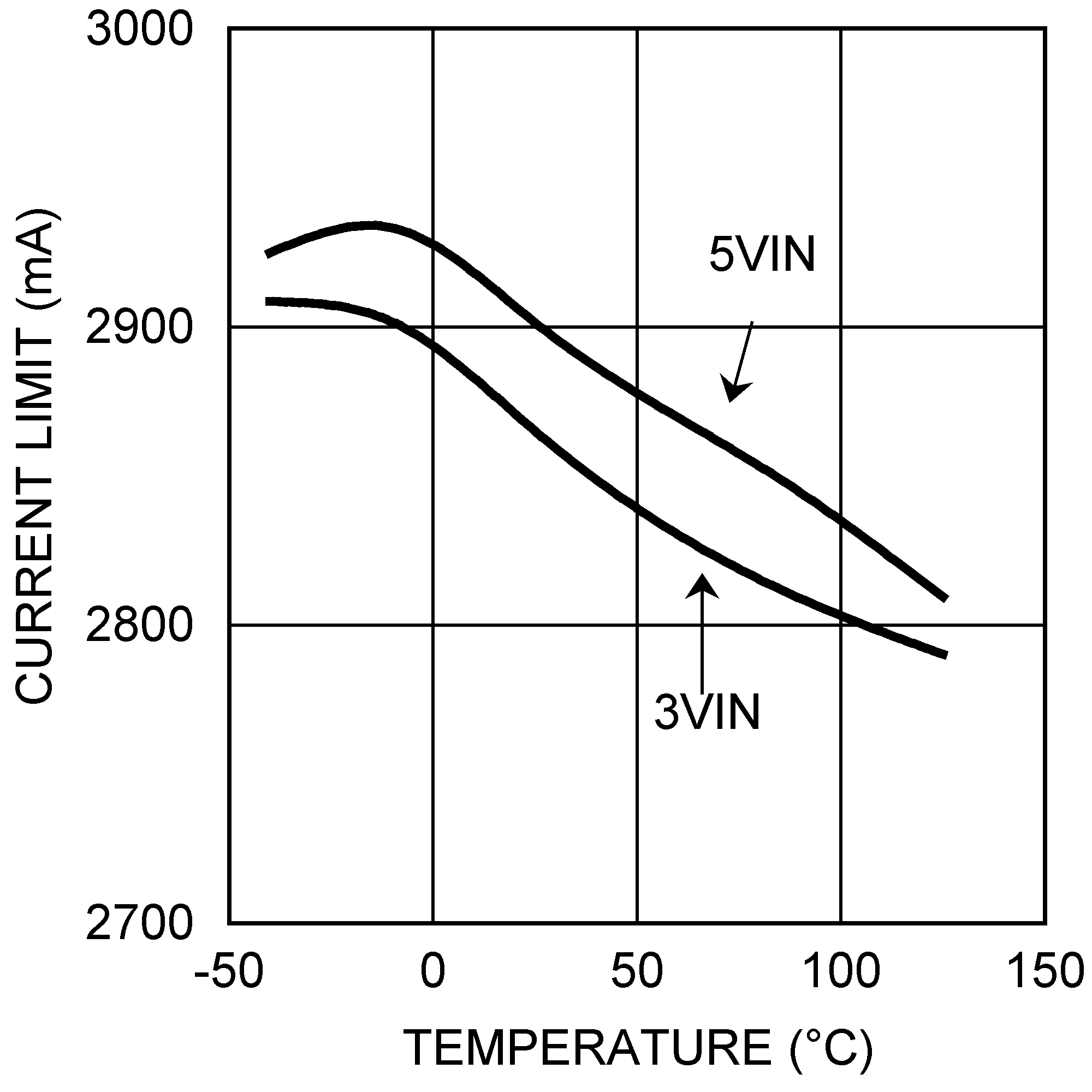 Figure 5. Current Limit vs Temperature
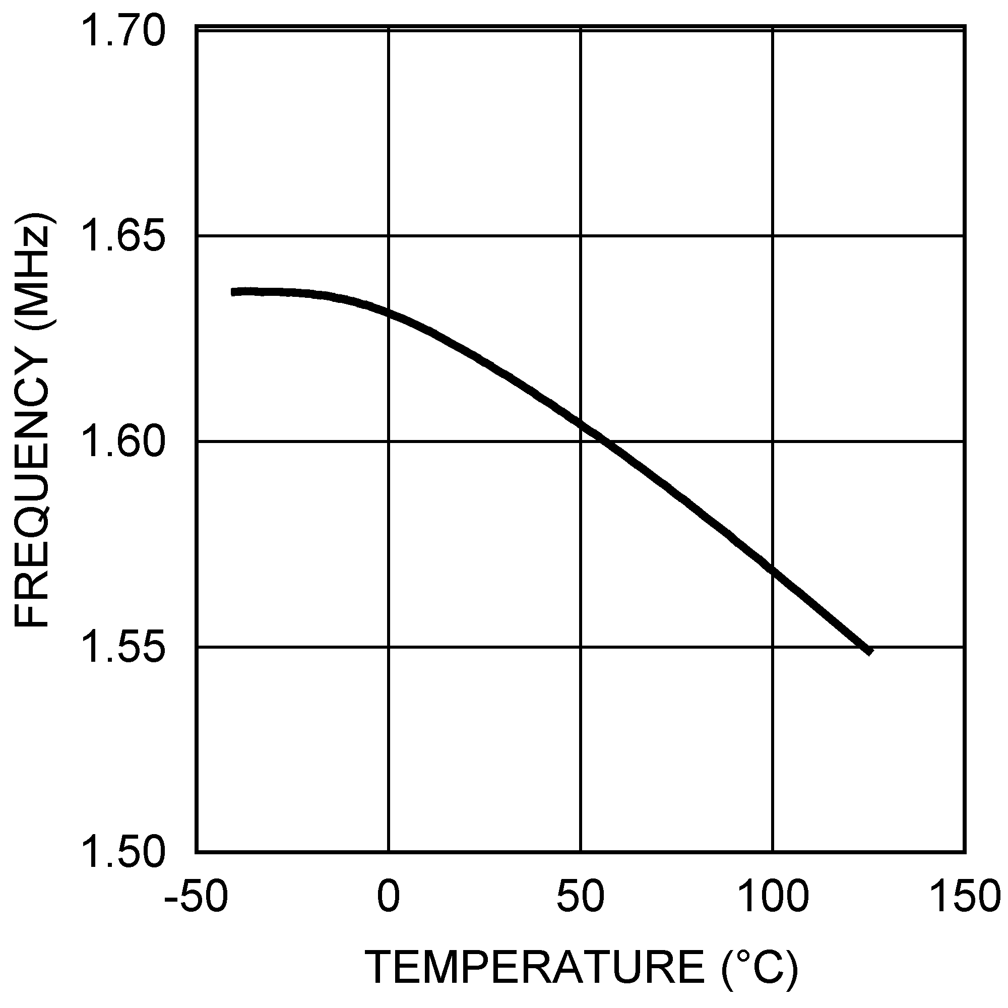
| LM3410X |
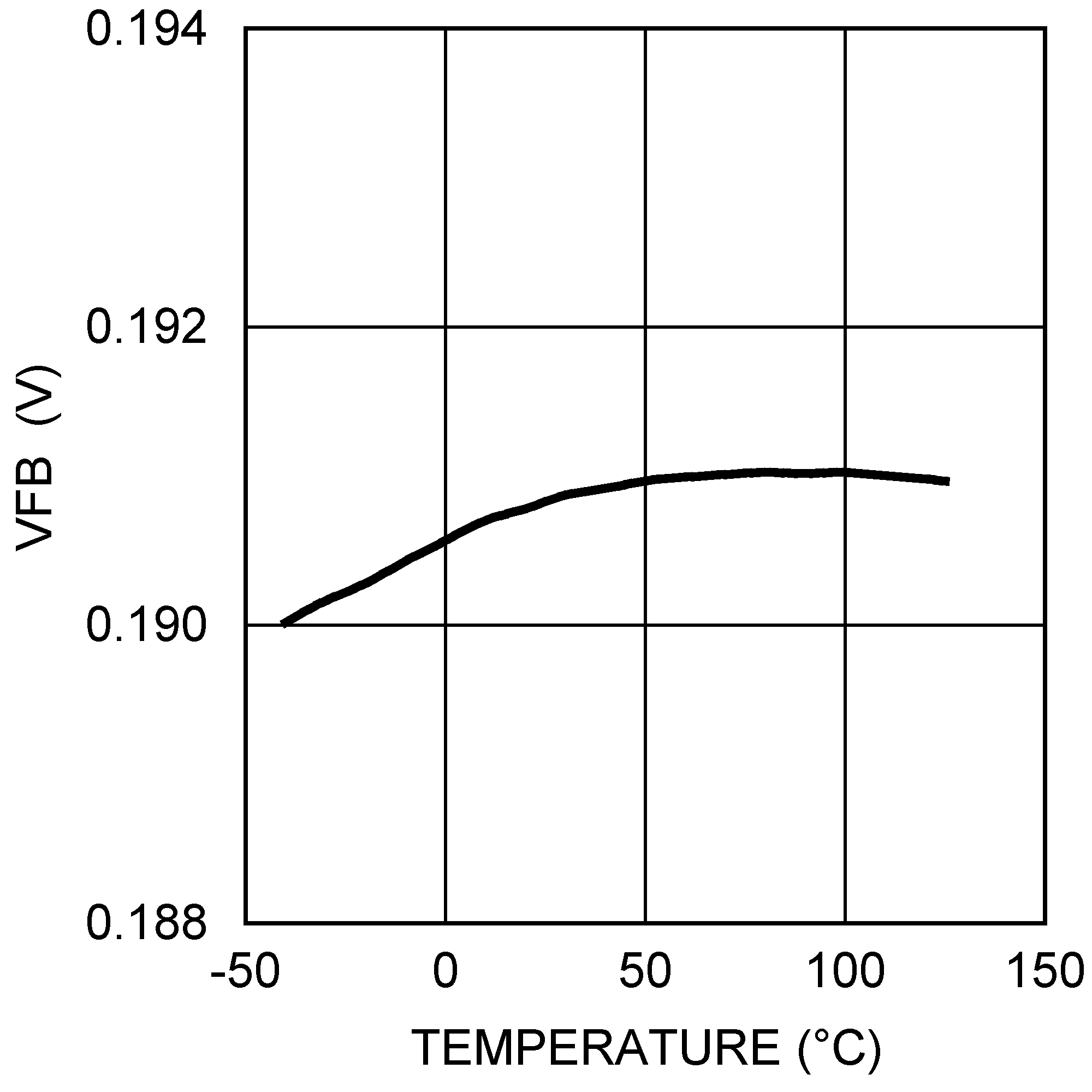 Figure 9. VFB vs Temperature
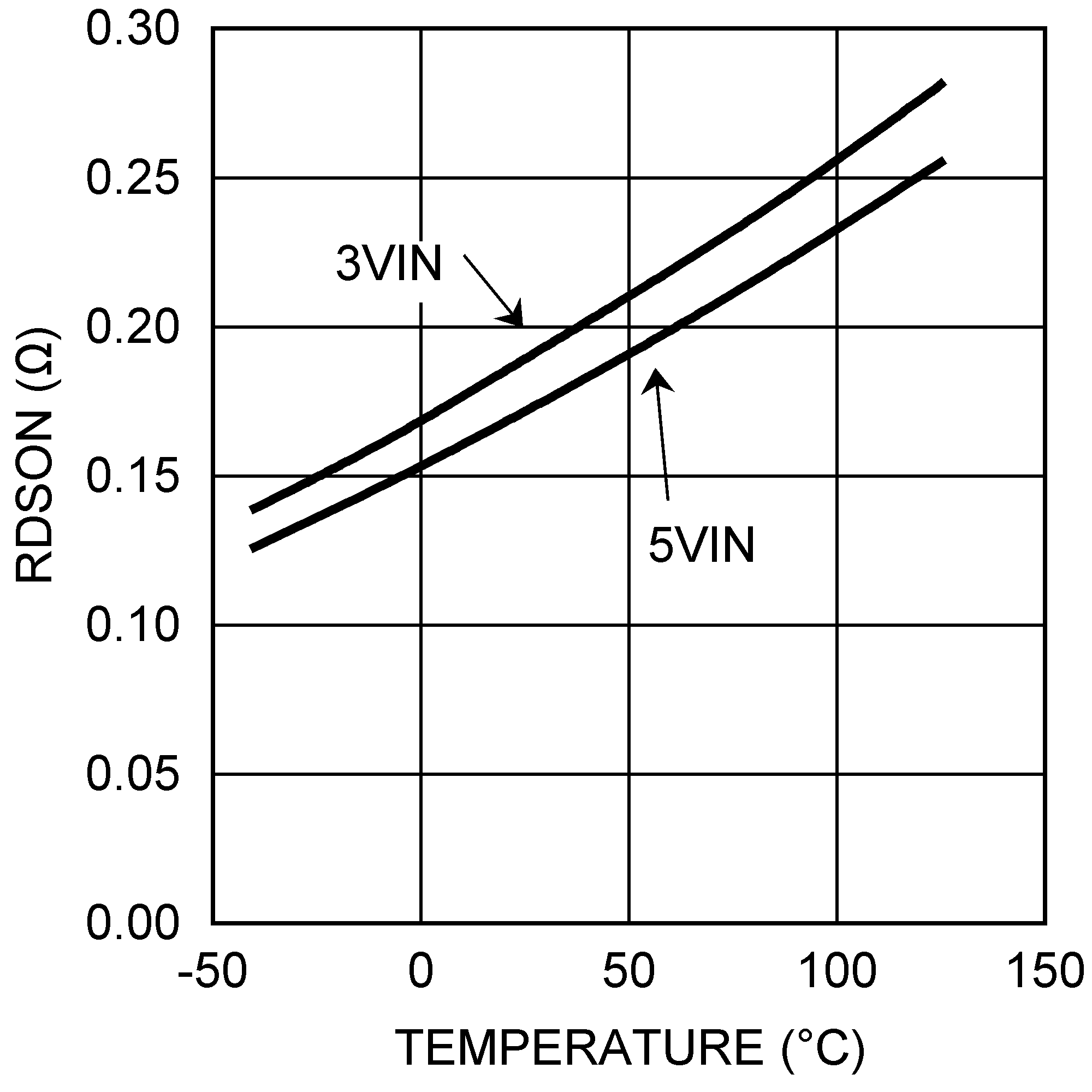 Figure 6. RDS(ON) vs Temperature
| LM3410Y |