JAJSHR8G July 2008 – July 2019 LM3421 , LM3423
PRODUCTION DATA.
- 1 特長
- 2 アプリケーション
- 3 概要
- 4 改訂履歴
- 5 Device Comparison
- 6 Pin Configuration and Functions
- 7 Specifications
-
8 Detailed Description
- 8.1 Overview
- 8.2 Functional Block Diagram
- 8.3
Feature Description
- 8.3.1 Current Regulators
- 8.3.2 Predictive Off-Time (PRO) Control
- 8.3.3 Average LED Current
- 8.3.4 Analog Dimming
- 8.3.5 Current Sense and Current Limit
- 8.3.6 Overcurrent Protection
- 8.3.7 Zero Current Shutdown
- 8.3.8 Control Loop Compensation
- 8.3.9 Start-Up Regulator
- 8.3.10 Overvoltage Lockout (OVLO)
- 8.3.11 Input Undervoltage Lockout (UVLO)
- 8.3.12 PWM Dimming
- 8.3.13 LM3423 Only: DPOL, FLT, TIMR, and LRDY
-
9 Application and Implementation
- 9.1 Application Information
- 9.2
Typical Applications
- 9.2.1
Basic Topology Schematics
- 9.2.1.1 Design Requirements
- 9.2.1.2
Detailed Design Procedure
- 9.2.1.2.1 Operating Point
- 9.2.1.2.2 Switching Frequency
- 9.2.1.2.3 Average LED Current
- 9.2.1.2.4 Inductor Ripple Current
- 9.2.1.2.5 LED Ripple Current
- 9.2.1.2.6 Peak Current Limit
- 9.2.1.2.7 Loop Compensation
- 9.2.1.2.8 Input Capacitance
- 9.2.1.2.9 N-channel FET
- 9.2.1.2.10 Diode
- 9.2.1.2.11 Output OVLO
- 9.2.1.2.12 Input UVLO
- 9.2.1.2.13 PWM Dimming Method
- 9.2.1.2.14 Analog Dimming Method
- 9.2.2
LM3421 Buck-Boost Application
- 9.2.2.1 Design Requirements
- 9.2.2.2
Detailed Design Procedure
- 9.2.2.2.1 Operating Point
- 9.2.2.2.2 Switching Frequency
- 9.2.2.2.3 Average LED Current
- 9.2.2.2.4 Inductor Ripple Current
- 9.2.2.2.5 Output Capacitance
- 9.2.2.2.6 Peak Current Limit
- 9.2.2.2.7 Loop Compensation
- 9.2.2.2.8 Input Capacitance
- 9.2.2.2.9 N-channel FET
- 9.2.2.2.10 Diode
- 9.2.2.2.11 Input UVLO
- 9.2.2.2.12 Output OVLO
- 9.2.2.3 Application Curve
- 9.2.3 LM3421 BOOST Application
- 9.2.4 LM3421 Buck-Boost Application
- 9.2.5 LM3423 Boost Application
- 9.2.6 LM3421 Buck-Boost Application
- 9.2.7 LM3423 Buck Application
- 9.2.8 LM3423 Buck-Boost Application
- 9.2.9 LM3421 SEPIC Application
- 9.2.1
Basic Topology Schematics
- 10Power Supply Recommendations
- 11Layout
- 12デバイスおよびドキュメントのサポート
- 13メカニカル、パッケージ、および注文情報
パッケージ・オプション
メカニカル・データ(パッケージ|ピン)
- PWP|16
サーマルパッド・メカニカル・データ
- PWP|16
発注情報
8.3.3 Average LED Current
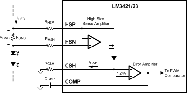
 Figure 13. LED Current Sense Circuitry
 The LM3421 and LM3423 use an external current sense resistor (RSNS) placed in series with the LED load to convert the LED current (ILED) into a voltage (VSNS) as shown in Figure 13. The HSP and HSN pins are the inputs to the high-side sense amplifier which are forced to be equal potential (VHSP=VHSN) through negative feedback. Because of this, the VSNS voltage is forced across RHSP to generate the signal current (ICSH) which flows out of the CSH pin and through the RCSH resistor. The error amplifier regulates the CSH pin to 1.24 V, therefore ICSH can be calculated using Equation 4.

This application regulates VSNS as described in Equation 5.

Calculate ILED using Equation 6.

The selection of the three resistors (RSNS, RCSH, and RHSP) is not arbitrary. For matching and noise performance, the suggested signal current ICSH is approximately 100 µA. This current does not flow in the LEDs and does not affect either the off-state LED current or the regulated LED current. ICSH can be above or below this value, but the high-side amplifier offset characteristics may be affected slightly. In addition, to minimize the effect of the high-side amplifier voltage offset on LED current accuracy, the minimum VSNS is suggested to be 50 mV. Place a resistor (RHSN = RHSP) in series with the HSN pin to cancel out the effects of the input bias current (approximately 10 µA) of both inputs of the high-side sense amplifier.
The sense resistor (RSNS) can be placed anywhere in the series string of LEDs as long as the voltage at the HSN and HSP pins (VHSP and VHSN) satisfies the following conditions.

Typically, for a buck-boost configuration, RSNS is placed at the bottom of the string (LED-) which allows for greater flexibility of input and output voltage. However, if there is substantial input voltage ripple allowed, it can help to place RSNS at the top of the string (LED+) which limits the output voltage of the string to:

The CSH pin can also be used as a low-side current sense input regulated to 1.24 V. The high-side sense amplifier is disabled if HSP and HSN are tied to AGND (or VHSN > VHSP) .