JAJSHR8G July 2008 – July 2019 LM3421 , LM3423
PRODUCTION DATA.
- 1 特長
- 2 アプリケーション
- 3 概要
- 4 改訂履歴
- 5 Device Comparison
- 6 Pin Configuration and Functions
- 7 Specifications
-
8 Detailed Description
- 8.1 Overview
- 8.2 Functional Block Diagram
- 8.3
Feature Description
- 8.3.1 Current Regulators
- 8.3.2 Predictive Off-Time (PRO) Control
- 8.3.3 Average LED Current
- 8.3.4 Analog Dimming
- 8.3.5 Current Sense and Current Limit
- 8.3.6 Overcurrent Protection
- 8.3.7 Zero Current Shutdown
- 8.3.8 Control Loop Compensation
- 8.3.9 Start-Up Regulator
- 8.3.10 Overvoltage Lockout (OVLO)
- 8.3.11 Input Undervoltage Lockout (UVLO)
- 8.3.12 PWM Dimming
- 8.3.13 LM3423 Only: DPOL, FLT, TIMR, and LRDY
-
9 Application and Implementation
- 9.1 Application Information
- 9.2
Typical Applications
- 9.2.1
Basic Topology Schematics
- 9.2.1.1 Design Requirements
- 9.2.1.2
Detailed Design Procedure
- 9.2.1.2.1 Operating Point
- 9.2.1.2.2 Switching Frequency
- 9.2.1.2.3 Average LED Current
- 9.2.1.2.4 Inductor Ripple Current
- 9.2.1.2.5 LED Ripple Current
- 9.2.1.2.6 Peak Current Limit
- 9.2.1.2.7 Loop Compensation
- 9.2.1.2.8 Input Capacitance
- 9.2.1.2.9 N-channel FET
- 9.2.1.2.10 Diode
- 9.2.1.2.11 Output OVLO
- 9.2.1.2.12 Input UVLO
- 9.2.1.2.13 PWM Dimming Method
- 9.2.1.2.14 Analog Dimming Method
- 9.2.2
LM3421 Buck-Boost Application
- 9.2.2.1 Design Requirements
- 9.2.2.2
Detailed Design Procedure
- 9.2.2.2.1 Operating Point
- 9.2.2.2.2 Switching Frequency
- 9.2.2.2.3 Average LED Current
- 9.2.2.2.4 Inductor Ripple Current
- 9.2.2.2.5 Output Capacitance
- 9.2.2.2.6 Peak Current Limit
- 9.2.2.2.7 Loop Compensation
- 9.2.2.2.8 Input Capacitance
- 9.2.2.2.9 N-channel FET
- 9.2.2.2.10 Diode
- 9.2.2.2.11 Input UVLO
- 9.2.2.2.12 Output OVLO
- 9.2.2.3 Application Curve
- 9.2.3 LM3421 BOOST Application
- 9.2.4 LM3421 Buck-Boost Application
- 9.2.5 LM3423 Boost Application
- 9.2.6 LM3421 Buck-Boost Application
- 9.2.7 LM3423 Buck Application
- 9.2.8 LM3423 Buck-Boost Application
- 9.2.9 LM3421 SEPIC Application
- 9.2.1
Basic Topology Schematics
- 10Power Supply Recommendations
- 11Layout
- 12デバイスおよびドキュメントのサポート
- 13メカニカル、パッケージ、および注文情報
パッケージ・オプション
メカニカル・データ(パッケージ|ピン)
- PWP|16
サーマルパッド・メカニカル・データ
- PWP|16
発注情報
8.3.13 LM3423 Only: DPOL, FLT, TIMR, and LRDY
The LM3423 has four additional pins: DPOL, FLT, TIMR, and LRDY. The DPOL pin is simply used to invert the DDRV polarity . If DPOL is left open, then it is internally pulled high and the polarity is correct for driving a series N-channel dimFET. If DPOL is pulled low then the polarity is correct for using a series P-channel dimFET in high-side dimming applications. For a parallel P-channel dimFET, as used in the buck topology, leave DPOL open for proper polarity.
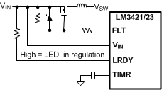
The additional TIMR and FLT pins can be used in conjunction with an input disconnect MOSFET switch as shown in Figure 28 to protect the module from various fault conditions.
A fault is detected and an 11.5 µA (typical) current is sourced from the TIMR pin whenever any one of the following conditions exists.
- LED current is above regulation by more than 30%.
- OVLO has engaged.
- Thermal shutdown has engaged.
An external capacitor (CTMR) from TIMR to AGND programs the fault filter time as follows:

When the voltage on the TIMR pin reaches 1.24 V, the device is latched off and the N-channel MOSFET open-drain FLT pin transitions to a high impedance state. The controller immediatly pulls the TIMR pin to ground (resets) if the fault condition is removed at any point during the filter period. Otherwise, if the timer expires, the fault remains latched until one of these situations occurs:
- The EN pin is pulled low long enough for the VCC pin to drop below 4.1 V (approximately 200 ms) or
- the TIMR pin is pulled to ground or
- a complete power cycle occurs
When using the EN and OVP pins in conjunction with the RPD pulldown pin, a race condition exists when exiting the disabled (EN low) state. When disabled, controller pulls up the OVP pin to the output voltage because the RPD pulldown is disabled, and this appears as if it is a real OVLO condition. The timer pin immediately rises and latches the controller to the fault state. To protect against this behavior, a minimum timer capacitor (CTMR = 220 pF) should be used. If fault latching is not required, short the TMR pin to AGND, which disables the FLT flag function.
The LM3423 also includes an LED Ready (LRDY) flag to notify the system that the LEDs are in proper regulation. The N-channel MOSFET open-drain LRDY pin is pulled low whenever any of the following conditions are met:
- VCC UVLO has engaged.
- LED current is below regulation by more than 20%.
- LED current is above regulation by more than 30%.
- Overvoltage protection has engaged
- Thermal shutdown has engaged.
- A fault has latched the device off.
The LRDY pin is pulled low during start-up of the device and remains low until the LED current is in regulation.
 Figure 28. Fault Detection and LED Status Circuit