JAJSHR8G July 2008 – July 2019 LM3421 , LM3423
PRODUCTION DATA.
- 1 特長
- 2 アプリケーション
- 3 概要
- 4 改訂履歴
- 5 Device Comparison
- 6 Pin Configuration and Functions
- 7 Specifications
-
8 Detailed Description
- 8.1 Overview
- 8.2 Functional Block Diagram
- 8.3
Feature Description
- 8.3.1 Current Regulators
- 8.3.2 Predictive Off-Time (PRO) Control
- 8.3.3 Average LED Current
- 8.3.4 Analog Dimming
- 8.3.5 Current Sense and Current Limit
- 8.3.6 Overcurrent Protection
- 8.3.7 Zero Current Shutdown
- 8.3.8 Control Loop Compensation
- 8.3.9 Start-Up Regulator
- 8.3.10 Overvoltage Lockout (OVLO)
- 8.3.11 Input Undervoltage Lockout (UVLO)
- 8.3.12 PWM Dimming
- 8.3.13 LM3423 Only: DPOL, FLT, TIMR, and LRDY
-
9 Application and Implementation
- 9.1 Application Information
- 9.2
Typical Applications
- 9.2.1
Basic Topology Schematics
- 9.2.1.1 Design Requirements
- 9.2.1.2
Detailed Design Procedure
- 9.2.1.2.1 Operating Point
- 9.2.1.2.2 Switching Frequency
- 9.2.1.2.3 Average LED Current
- 9.2.1.2.4 Inductor Ripple Current
- 9.2.1.2.5 LED Ripple Current
- 9.2.1.2.6 Peak Current Limit
- 9.2.1.2.7 Loop Compensation
- 9.2.1.2.8 Input Capacitance
- 9.2.1.2.9 N-channel FET
- 9.2.1.2.10 Diode
- 9.2.1.2.11 Output OVLO
- 9.2.1.2.12 Input UVLO
- 9.2.1.2.13 PWM Dimming Method
- 9.2.1.2.14 Analog Dimming Method
- 9.2.2
LM3421 Buck-Boost Application
- 9.2.2.1 Design Requirements
- 9.2.2.2
Detailed Design Procedure
- 9.2.2.2.1 Operating Point
- 9.2.2.2.2 Switching Frequency
- 9.2.2.2.3 Average LED Current
- 9.2.2.2.4 Inductor Ripple Current
- 9.2.2.2.5 Output Capacitance
- 9.2.2.2.6 Peak Current Limit
- 9.2.2.2.7 Loop Compensation
- 9.2.2.2.8 Input Capacitance
- 9.2.2.2.9 N-channel FET
- 9.2.2.2.10 Diode
- 9.2.2.2.11 Input UVLO
- 9.2.2.2.12 Output OVLO
- 9.2.2.3 Application Curve
- 9.2.3 LM3421 BOOST Application
- 9.2.4 LM3421 Buck-Boost Application
- 9.2.5 LM3423 Boost Application
- 9.2.6 LM3421 Buck-Boost Application
- 9.2.7 LM3423 Buck Application
- 9.2.8 LM3423 Buck-Boost Application
- 9.2.9 LM3421 SEPIC Application
- 9.2.1
Basic Topology Schematics
- 10Power Supply Recommendations
- 11Layout
- 12デバイスおよびドキュメントのサポート
- 13メカニカル、パッケージ、および注文情報
パッケージ・オプション
メカニカル・データ(パッケージ|ピン)
- PWP|16
サーマルパッド・メカニカル・データ
- PWP|16
発注情報
9.1.8 Switching Frequency
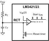
An external resistor (RT) connected between the RCT pin and the switch node (where D1, Q1, and L1 connect), in combination with a capacitor (CT) between the RCT and AGND pins, sets the off-time (tOFF) as shown in Figure 31. For boost and buck-boost topologies, the VIN proportionality ensures a virtually constant switching frequency (fSW).
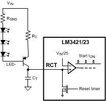
For a buck topology, RT and CT are also used to set tOFF, however the iinput voltage (VIN) proportionality does not ensure a constant switching frequency. Instead, constant ripple operation can be achieved. Changing the connection of RT in Figure 31 from VSW to VIN provides a constant ripple over varying VIN. Adding a PNP transistor as shown in Figure 32 provides constant ripple over varying VO.
The switching frequency is defined:
Buck (Constant Ripple vs. VIN)

Buck (Constant Ripple vs. VO)

Boost and Buck-boost

For all topologies, the CT capacitor is recommended to be 1 nF and should be located very close to the LM34xx-Q1.
 Figure 31. Off-timer Circuitry for Boost and Buck-boost Regulators
  Figure 32. Off-timer Circuitry for Buck Regulators