JAJSHR8G July 2008 – July 2019 LM3421 , LM3423
PRODUCTION DATA.
- 1 特長
- 2 アプリケーション
- 3 概要
- 4 改訂履歴
- 5 Device Comparison
- 6 Pin Configuration and Functions
- 7 Specifications
-
8 Detailed Description
- 8.1 Overview
- 8.2 Functional Block Diagram
- 8.3
Feature Description
- 8.3.1 Current Regulators
- 8.3.2 Predictive Off-Time (PRO) Control
- 8.3.3 Average LED Current
- 8.3.4 Analog Dimming
- 8.3.5 Current Sense and Current Limit
- 8.3.6 Overcurrent Protection
- 8.3.7 Zero Current Shutdown
- 8.3.8 Control Loop Compensation
- 8.3.9 Start-Up Regulator
- 8.3.10 Overvoltage Lockout (OVLO)
- 8.3.11 Input Undervoltage Lockout (UVLO)
- 8.3.12 PWM Dimming
- 8.3.13 LM3423 Only: DPOL, FLT, TIMR, and LRDY
-
9 Application and Implementation
- 9.1 Application Information
- 9.2
Typical Applications
- 9.2.1
Basic Topology Schematics
- 9.2.1.1 Design Requirements
- 9.2.1.2
Detailed Design Procedure
- 9.2.1.2.1 Operating Point
- 9.2.1.2.2 Switching Frequency
- 9.2.1.2.3 Average LED Current
- 9.2.1.2.4 Inductor Ripple Current
- 9.2.1.2.5 LED Ripple Current
- 9.2.1.2.6 Peak Current Limit
- 9.2.1.2.7 Loop Compensation
- 9.2.1.2.8 Input Capacitance
- 9.2.1.2.9 N-channel FET
- 9.2.1.2.10 Diode
- 9.2.1.2.11 Output OVLO
- 9.2.1.2.12 Input UVLO
- 9.2.1.2.13 PWM Dimming Method
- 9.2.1.2.14 Analog Dimming Method
- 9.2.2
LM3421 Buck-Boost Application
- 9.2.2.1 Design Requirements
- 9.2.2.2
Detailed Design Procedure
- 9.2.2.2.1 Operating Point
- 9.2.2.2.2 Switching Frequency
- 9.2.2.2.3 Average LED Current
- 9.2.2.2.4 Inductor Ripple Current
- 9.2.2.2.5 Output Capacitance
- 9.2.2.2.6 Peak Current Limit
- 9.2.2.2.7 Loop Compensation
- 9.2.2.2.8 Input Capacitance
- 9.2.2.2.9 N-channel FET
- 9.2.2.2.10 Diode
- 9.2.2.2.11 Input UVLO
- 9.2.2.2.12 Output OVLO
- 9.2.2.3 Application Curve
- 9.2.3 LM3421 BOOST Application
- 9.2.4 LM3421 Buck-Boost Application
- 9.2.5 LM3423 Boost Application
- 9.2.6 LM3421 Buck-Boost Application
- 9.2.7 LM3423 Buck Application
- 9.2.8 LM3423 Buck-Boost Application
- 9.2.9 LM3421 SEPIC Application
- 9.2.1
Basic Topology Schematics
- 10Power Supply Recommendations
- 11Layout
- 12デバイスおよびドキュメントのサポート
- 13メカニカル、パッケージ、および注文情報
パッケージ・オプション
メカニカル・データ(パッケージ|ピン)
- PWP|20
サーマルパッド・メカニカル・データ
- PWP|20
発注情報
8.3.4 Analog Dimming
The CSH pin can be used to analog dim the LED current by adjusting the current sense voltage (VSNS). There are several different methods to adjust VSNS using the CSH pin:
- External variable resistance: Adjust a potentiometer placed in series with RCSH to vary VSNS.
- External variable current source: Source current (0 µA to ICSH) into the CSH pin to adjust VSNS.
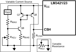
 Figure 14. Analog Dimming Circuitry
 In general, analog dimming applications require a lower switching frequency to minimize the effect of the leading edge blanking circuit. As the LED current is reduced, the output voltage and the duty cycle decreases. Eventually, the minimum on-time is reached. The lower the switching frequency, the wider the linear dimming range. Figure 14 shows how both CSH methods are physically implemented.
Method 1 uses an external potentiometer in the CSH path which is a simple addition to the existing circuitry. However, the LEDs cannot dim completely because there is always some resistance causing signal current to flow. This method is also susceptible to noise coupling at the CSH pin because the potentiometer increases the size of the signal current loop.
Method 2 provides a complete dimming range and better noise performance, though it is more complex. It consists of a PNP current mirror and a bias network consisting of an NPN, 2 resistors and a potentiometer (RADJ), where RADJ controls the amount of current sourced into the CSH pin. A higher resistance value sources more current into the CSH pin, causing less regulated signal current through RHSP, effectively dimming the LEDs. VREF should be a precise external voltage reference, while Q7 and Q8 should be a dual pair PNP for best matching and performance. The additional current (IADD) sourced into the CSH pin can be calculated using Equation 9.

The corresponding LED current ( ILED) for a specific IADD is:
