JAJS711X July 2000 – June 2017 LM3478
PRODUCTION DATA.
- 1 特長
- 2 アプリケーション
- 3 説明
- 4 改訂履歴
- 5 Pin Configuration and Functions
- 6 Specifications
- 7 Detailed Description
-
8 Application and Implementation
- 8.1 Application Information
- 8.2
Typical Applications
- 8.2.1
Typical High Efficiency Step-Up (Boost) Converter
- 8.2.1.1 Design Requirements
- 8.2.1.2
Detailed Design Procedure
- 8.2.1.2.1 Custom Design with WEBENCH Tools
- 8.2.1.2.2 Power Inductor Selection
- 8.2.1.2.3 Programming the Output Voltage
- 8.2.1.2.4 Setting the Current Limit
- 8.2.1.2.5 Current Limit with External Slope Compensation
- 8.2.1.2.6 Power Diode Selection
- 8.2.1.2.7 Power MOSFET Selection
- 8.2.1.2.8 Input Capacitor Selection
- 8.2.1.2.9 Output Capacitor Selection
- 8.2.1.2.10 Compensation
- 8.2.1.3 Application Curves
- 8.2.2 Typical SEPIC Converter
- 8.2.1
Typical High Efficiency Step-Up (Boost) Converter
- 9 Power Supply Recommendations
- 10Layout
- 11デバイスおよびドキュメントのサポート
- 12メカニカル、パッケージ、および注文情報
パッケージ・オプション
メカニカル・データ(パッケージ|ピン)
サーマルパッド・メカニカル・データ
発注情報
6 Specifications
6.1 Absolute Maximum Ratings
over operating free-air temperature (unless otherwise noted) (1)| MIN | MAX | UNIT | ||
|---|---|---|---|---|
| Input Voltage | 45 | V | ||
| FB Pin Voltage | –0.4< V | V FB < 7 | V | |
| FA/SD Pin Voltage | –0.4 < VFA/SD | VFA/SD< 7 | V | |
| Peak Driver Output Current (<10µs) | 1 | A | ||
| Power Dissipation | Internally Limited | |||
| Junction Temperature | +150 | °C | ||
| Lead Temperature | Vapor Phase (60 s) | 215 | °C | |
| Infrared (15 s) | 260 | °C | ||
| DR Pin Voltage | –0.4 ≤ VDR | VDR ≤ 8 | V | |
| ISEN Pin Voltage | 500 | mV | ||
| Tstg | Storage temperature | −65 | 150 | °C |
(1) Stresses beyond those listed under Absolute Maximum Ratings may cause permanent damage to the device. These are stress ratings only, which do not imply functional operation of the device at these or any other conditions beyond those indicated under Recommended Operating Conditions. Exposure to absolute-maximum-rated conditions for extended periods may affect device reliability.
6.2 ESD Ratings - LM3478
| VALUE | UNIT | ||||
|---|---|---|---|---|---|
| V(ESD) | Electrostatic discharge | Human body model (HBM), per ANSI/ESDA/JEDEC JS-001, all pins(1) | ±2000 | V | |
| Charged device model (CDM), per JEDEC specification JESD22-C101, all pins(2) | ±750 | ||||
(1) JEDEC document JEP155 states that 500-V HBM allows safe manufacturing with a standard ESD control process.
(2) JEDEC document JEP157 states that 250-V CDM allows safe manufacturing with a standard ESD control process.
6.3 Recommended Operating Conditions
over operating free-air temperature range (unless otherwise noted)| MIN | NOM | MAX | UNIT | ||
|---|---|---|---|---|---|
| Supply Voltage | 2.97 ≤ VIN | VIN ≤ 40 | V | ||
| Junction Temperature Range | −40 ≤ TJ | TJ ≤ +125 | °C | ||
| Switching Frequency | 100 ≤ FSW | FSW ≤ 1 | MHz | ||
6.4 Thermal Information
| THERMAL METRIC(1) | LM3478 | UNIT | ||
|---|---|---|---|---|
| D | DGK | |||
| 8 PINS | 8 PINS | |||
| RθJA | Junction-to-ambient thermal resistance | 105.3 | 157.2 | °C/W |
| RθJC(top) | Junction-to-case (top) thermal resistance | 50.3 | 49.9 | °C/W |
| RθJB | Junction-to-board thermal resistance | 55.8 | 77.1 | °C/W |
| ψJT | Junction-to-top characterization parameter | 6.8 | 4.7 | °C/W |
| ψJB | Junction-to-board characterization parameter | 54.7 | 75.8 | °C/W |
| RθJC(bot) | Junction-to-case (bottom) thermal resistance | N/A | N/A | °C/W |
(1) For more information about traditional and new thermal metrics, see the IC Package Thermal Metrics application report, SPRA953.
6.5 Electrical Characteristics
Unless otherwise specified, VIN = 12V, RFA = 40kΩ, TJ = 25°C| PARAMETER | TEST CONDITIONS | MIN | TYP | MAX | UNIT | |
|---|---|---|---|---|---|---|
| VFB | Feedback Voltage | VCOMP = 1.4V, 2.97 ≤ VIN ≤ 40V | 1.2416 | 1.26 | 1.2843 | V |
| VCOMP = 1.4V, 2.97 ≤ VIN ≤ 40V, −40°C ≤ TJ ≤ 125°C | 1.228 | 1.292 | ||||
| ΔVLINE | Feedback Voltage Line Regulation | 2.97 ≤ VIN ≤ 40V | 0.001 | %/V | ||
| ΔVLOAD | Output Voltage Load Regulation | IEAO Source/Sink | ±0.5 | %/A | ||
| VUVLO | Input Undervoltage Lock-out | 2.85 | V | |||
| −40°C ≤ TJ ≤ 125°C | 2.97 | |||||
| VUV(HYS) | Input Undervoltage Lock-out Hysteresis | 170 | mV | |||
| −40°C ≤ TJ ≤ 125°C | 130 | 210 | ||||
| Fnom | Nominal Switching Frequency | RFA = 40KΩ | 400 | kHz | ||
| RFA = 40KΩ, −40°C ≤ TJ ≤ 125°C | 350 | 440 | ||||
| RDS1 (ON) | Driver Switch On Resistance (top) | IDR = 0.2A, VIN= 5V | 16 | Ω | ||
| RDS2 (ON) | Driver Switch On Resistance (bottom) | IDR = 0.2A | 4.5 | |||
| VDR (max) | Maximum Drive Voltage Swing(2) | VIN < 7.2V | VIN | V | ||
| VIN ≥ 7.2V | 7.2 | |||||
| Dmax | Maximum Duty Cycle(3) | 100% | ||||
| Tmin (on) | Minimum On Time | 325 | ns | |||
| −40°C ≤ TJ ≤ 125°C | 210 | 600 | ||||
| ISUPPLY | Supply Current (non-switching) | See (5) | 2.7 | mA | ||
| See (5), −40°C ≤ TJ ≤ 125°C | 3.3 | |||||
| IQ | Quiescent Current in Shutdown Mode | VFA/SD = 5V (6), VIN = 5V | 5 | µA | ||
| VFA/SD = 5V (6), VIN = 5V, −40°C ≤ TJ ≤ 125°C | 10 | |||||
| VSENSE | Current Sense Threshold Voltage | VIN = 5V | 135 | 156 | 180 | mV |
| VIN = 5V, −40°C ≤ TJ ≤ 125°C | 125 | 190 | ||||
| VSC | Short-Circuit Current Limit Sense Voltage | VIN = 5V | 343 | mV | ||
| VIN = 5V, −40°C ≤ TJ ≤ 125°C | 250 | 415 | ||||
| VSL | Internal Compensation Ramp Voltage | VIN = 5V | 92 | mV | ||
| VIN = 5V, −40°C ≤ TJ ≤ 125°C | 52 | 132 | ||||
| VSL ratio | VSL/VSENSE | 0.30 | 0.49 | 0.70 | ||
| VOVP | Output Over-voltage Protection (with respect to feedback voltage) (4) | VCOMP = 1.4V | 32 | 50 | mV | |
| VCOMP = 1.4V, −40°C ≤ TJ ≤ 125°C | 25 | |||||
| VSSOP Package | 78 | |||||
| VSSOP Package, −40°C ≤ TJ ≤ 125°C | 85 | |||||
| SOIC Package | 78 | |||||
| SOIC Package, −40°C ≤ TJ ≤ 125°C | 100 | |||||
| VOVP(HYS) | Output Over-Voltage Protection Hysteresis(4) | VCOMP = 1.4V | 60 | mV | ||
| VCOMP = 1.4V, −40°C ≤ TJ ≤ 125°C | 20 | 110 | ||||
| Gm | Error Amplifier Transconductance | VCOMP = 1.4V, IEAO = 100µA (Source/Sink) | 600 | 800 | 1000 | µS |
| VCOMP = 1.4V, IEAO = 100µA (Source/Sink), −40°C ≤ TJ ≤ 125°C | 365 | 1265 | ||||
| AVOL | Error Amplifier Voltage Gain | VCOMP = 1.4V, IEAO = 100µA (Source/Sink) | 38 | V/V | ||
| VCOMP = 1.4V, IEAO = 100µA (Source/Sink), −40°C ≤ TJ ≤ 125°C | 26 | 44 | ||||
| IEAO | Error Amplifier Output Current (Source/ Sink) | Source, VCOMP = 1.4V, VFB = 0V | 80 | 110 | 140 | µA |
| Source, VCOMP = 1.4V, VFB = 0V, −40°C ≤ TJ ≤ 125°C | 50 | 180 | ||||
| Sink, VCOMP = 1.4V, VFB = 1.4V | −100 | −140 | −180 | µA | ||
| Sink, VCOMP = 1.4V, VFB = 1.4V, −40°C ≤ TJ ≤ 125°C | −85 | −185 | ||||
| VEAO | Error Amplifier Output Voltage Swing | Upper Limit, VFB = 0V, COMP Pin = Floating | 2.2 | V | ||
| Upper Limit, VFB = 0V, COMP Pin = Floating, −40°C ≤ TJ ≤ 125°C | 1.8 | 2.4 | ||||
| Lower Limit, VFB = 1.4V | 0.56 | V | ||||
| Lower Limit, VFB = 1.4V, −40°C ≤ TJ ≤ 125°C | 0.2 | 1.0 | ||||
| TSS | Internal Soft-Start Delay | VFB = 1.2V, VCOMP = Floating | 4 | ms | ||
| Tr | Drive Pin Rise Time | Cgs = 3000pf, VDR = 0 to 3V | 25 | ns | ||
| Tf | Drive Pin Fall Time | Cgs = 3000pf, VDR = 0 to 3V | 25 | ns | ||
| VSD | Shutdown threshold (1) | Output = High | 1.27 | V | ||
| Output = High, −40°C ≤ TJ ≤ 125°C | 1.4 | |||||
| Output = Low | 0.65 | V | ||||
| Output = Low, −40°C ≤ TJ ≤ 125°C | 0.3 | |||||
| ISD | Shutdown Pin Current | VSD = 5V | −1 | µA | ||
| VSD = 0V | +1 | |||||
| IFB | Feedback Pin Current | 15 | nA | |||
| TSD | Thermal Shutdown | 165 | °C | |||
| Tsh | Thermal Shutdown Hysteresis | 10 | °C | |||
(1) The FA/SD pin should be pulled to VIN through a resistor to turn the regulator off. The voltage on the FA/SD pin must be above the maximum limit for Output = High to keep the regulator off and must be below the limit for Output = Low to keep the regulator on.
(2) The voltage on the drive pin, VDR is equal to the input voltage when input voltage is less than 7.2 V. VDR is equal to 7.2 V when the input voltage is greater than or equal to 7.2 V.
(3) The limits for the maximum duty cycle can not be specified since the part does not permit less than 100% maximum duty cycle operation.
(4) The over-voltage protection is specified with respect to the feedback voltage. This is because the over-voltage protection tracks the feedback voltage. The overvoltage protection threshold is given by adding the feedback voltage, VFB to the over-voltage protection specification.
(5) For this test, the FA/SD pin is pulled to ground using a 40-K resistor.
(6) For this test, the FA/SD pin is pulled to 5 V using a 40-K resistor.
6.6 Typical Characteristics
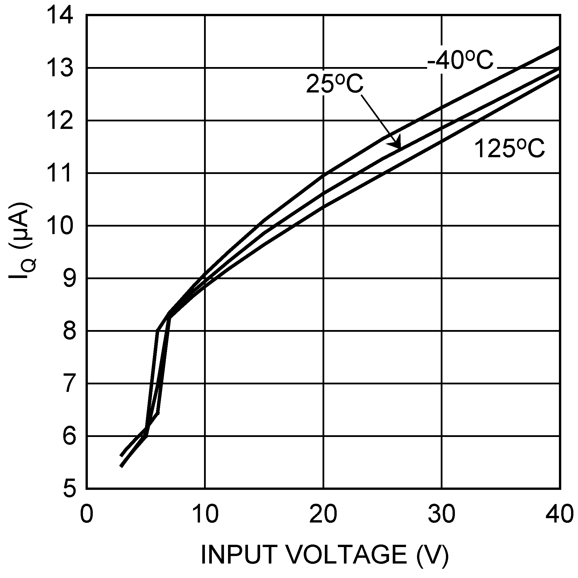
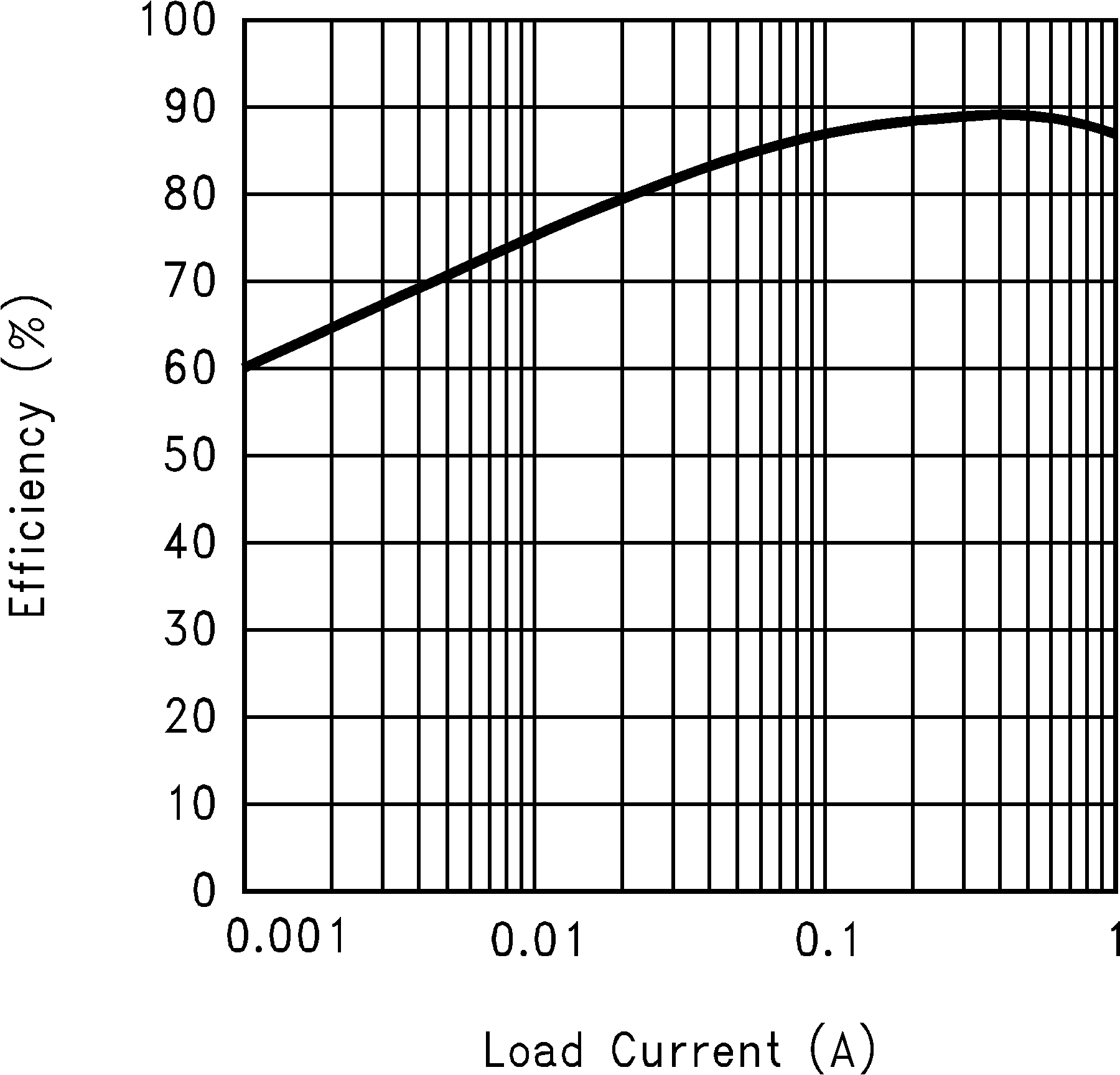
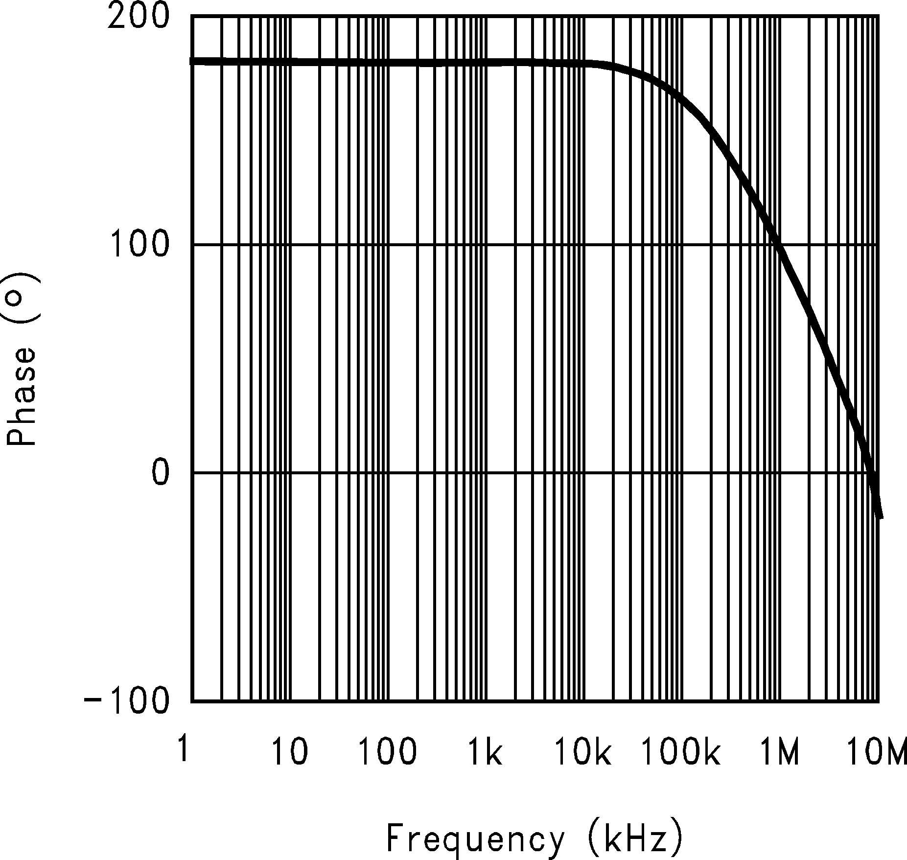
Unless otherwise specified, VIN = 12V, TJ = 25°C.


