SNOSC68C April 2012 – September 2015 LM3533
PRODUCTION DATA.
- 1 Features
- 2 Applications
- 3 Description
- 4 Revision History
- 5 Pin Configuration and Functions
- 6 Specifications
-
7 Detailed Description
- 7.1 Overview
- 7.2 Functional Block Diagram
- 7.3 Feature Description
- 7.4
Device Functional Modes
- 7.4.1 High-Voltage Boost Converter
- 7.4.2 Integrated Charge Pump
- 7.4.3 LED Current Mapping Modes
- 7.4.4 LED Current Ramping
- 7.4.5 Brightness Register Current Control
- 7.4.6 PWM Control
- 7.4.7 ALS Current Control
- 7.4.8
ALS Functional Blocks
- 7.4.8.1 ALS Input
- 7.4.8.2 Analog Output Ambient Light Sensors (ALS Gain Setting Resistors)
- 7.4.8.3 PWM Output Ambient Light Sensors (Internal Filtering)
- 7.4.8.4 Internal 8-Bit ADC
- 7.4.8.5 ALS Averager
- 7.4.8.6 Initializing the ALS
- 7.4.8.7 ALS Algorithms
- 7.4.8.8 ALS Rules
- 7.4.8.9 Direct ALS Control
- 7.4.8.10 Up-Only Control
- 7.4.8.11 Down-Delay Control
- 7.4.9 Pattern Generator
- 7.4.10 Fault Flags/Protection Features
- 7.5 Programming
- 7.6 Register Maps
- 8 Application and Implementation
- 9 Power Supply Recommendations
- 10Layout
- 11Device and Documentation Support
- 12Mechanical, Packaging, and Orderable Information
8 Application and Implementation
NOTE
Information in the following applications sections is not part of the TI component specification, and TI does not warrant its accuracy or completeness. TI’s customers are responsible for determining suitability of components for their purposes. Customers should validate and test their design implementation to confirm system functionality.
8.1 Application Information
The LM3533 is a dual-string (up to 40 V at up to 30 mA) backlight driver with five integrated low voltage indicator current sinks. The current through any LED can be controlled by the I2C bus, the PWM input, or via an external ambient light sensor. Any low voltage current sink can be made to blink via a programmable pattern. The programmable pattern can have variable high pulse time, low pulse time, delay from start, high time current, low time current, and ramp rates. The device operates from a typical VIN from 2.7 V to 5.5 V, and an ambient temperature range of -40°C to +85°C.
8.2 Typical Application
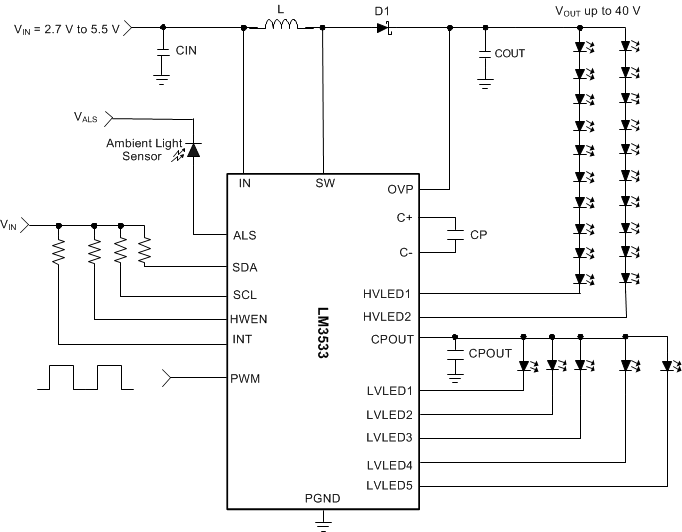 Figure 37. LM3533 Typical Application
8.2.1 Design Requirements
For typical lighting power-source applications, use the parameters listed in Table 48.
Table 48. Design Parameters
| DESIGN PARAMETER | EXAMPLE VALUE |
|---|---|
| Minimum input voltage | 2.7 V |
| Minimum output voltage | 0.6 V |
| Output current | 0 to 750 mA |
| Switching frequency | 2.4 MHz (typical) |
8.2.2 Detailed Design Procedure
Table 49. Application Circuit Component List
| COMPONENT | MANUFACTURER | VALUE | PART NUMBER | SIZE (mm) | CURRENT/VOLTAGE RATING (RESISTANCE) |
|---|---|---|---|---|---|
| L | TDK | 10 µH | VLF302512MT-100M | 2.5 x 3 x 1.2 | 620 mA/0.25 Ω |
| COUT | TDK | 1 µF | C2012X5R1H105 | 0805 | 50 V |
| CIN | TDK | 2.2 µF | C1005X5R1A225 | 0402 | 10 V |
| CPOUT/CP | TDK | 1 µF | C1005X5R1A105 | 0402 | 10 V |
| Diode | On-Semi | Schottky | NSR0240V2T1G | SOD-523 | 40 V, 250 mA |
8.2.2.1 Boost Converter Maximum Output Power (Boost)
The LM3533 maximum output power is governed by two factors: the peak current limit (ICL = 880 mA minimum), and the maximum output voltage (VOVP). When the application causes either of these limits to be reached, it is possible that the proper current regulation and matching between LED current strings may not be met.
8.2.2.2 Peak Current Limited
In the case of a peak current limited situation, when the peak of the inductor current hits the LM3533 current limit, the NFET switch turns off for the remainder of the switching period. If this happens each switching cycle the LM3533 regulates the peak of the inductor current instead of the headroom across the current sinks. This can result in the dropout of the boost output connected current sinks, and the LED current dropping below its programmed level.
The peak current in a boost converter is dependent on the value of the inductor, total LED current in the boost (IOUT), the boost output voltage (VOUT) (which is the highest voltage LED string + 0.4 V regulated headroom voltage), the input voltage (VIN), the switching frequency, and the efficiency (Output Power/Input Power). Additionally, the peak current is different depending on whether the inductor current is continuous during the entire switching period (CCM), or discontinuous (DCM) where it goes to 0 before the switching period ends. For Continuous Conduction Mode the peak inductor current is given by:

For DCM the peak inductor current is given by:

To determine which mode the circuit is operating in (CCM or DCM) it is necessary to perform a calculation to test whether the inductor current ripple is less than the anticipated input current (IIN). If ΔIL is less than IIN then the device is operating in CCM. If ΔIL is greater than IIN then the device is operating in DCM.

Typically at currents high enough to reach the LM3533 device's peak current limit, the device is operating in CCM. When choosing the switching frequency and the inductor value, Equation 16 and Equation 17 must be used to ensure that IPEAK stays below ICL_MIN (see Electrical Characteristics).
8.2.2.3 Output Voltage Limited
In the case of a output voltage limited situation, when the boost output voltage hits the LM3533 OVP threshold, the NFET turns off and stays off until the output voltage falls below the hysteresis level (typically 1 V below the OVP threshold). This results in the boost converter regulating the output voltage to the programmed OVP threshold (16 V, 24 V, 32 V, or 40 V), causing the current sinks to go into dropout. The default OVP threshold is set at 16 V. For LED strings higher than typically 4 series LEDs, the OVP has to be programmed higher after power-up or after a HWEN reset.
8.2.2.4 Maximum Output Power (Charge Pump)
The maximum output power available from the LM3533 charge pump is determined by the maximum output voltage available from the charge pump. In 1× gain the charge pump operates in Pass Mode so that the voltage at CPOUT tracks VIN (less the drop across the charge pumps pass switch). In this case the maximum output power is given as:

where
- RCP is the resistance from IN to CPOUT
- ILVLED_TOTAL is the maximum programmed current in the LVLED strings.
In 2× gain the voltage at CPOUT (VCPOUT_2X) is regulated to typically 4.4 V. In this case the maximum output power is given by:

Equation 19 and Equation 20 both assume there is sufficient headroom at the top side of the low-voltage current sinks to ensure the LED current remains in regulation (VHR_LV) in the Electrical Characteristics.
8.2.3 Application Curves
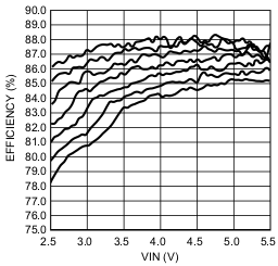
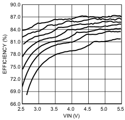
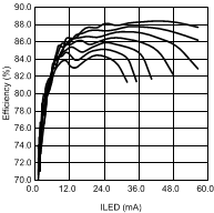
VIN = 3.6 V, LEDs are WLEDs part number SML-312WBCW(A), typical application circuit with L = TDK (VLF302512, 4.7 µH, 10 µH, 22 µH where specified), Schottky = On-Semi (NSR0240V2T1G), TA = 25°C, unless otherwise specified. Efficiency is given as VOUT × (IHVLED1 + IHVLED2)/(VIN × IIN); matching curves are given as (ΔILED_MAX/ILED_AVE).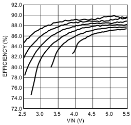
| L = 22 µH | 20 mA/String | ƒSW = 500 kHz |
| Top To Bottom: 2×4, 2×5, 2×6, 2×7, 2×8, 2×9 (LEDs) | ||
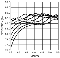
| L = 22 µH | 20 mA/String | ƒSW = 500 kHz |
| Top To Bottom: 1×4, 1×5, 1×6, 1×7, 1×8, 1×9, 1×10 (LEDs) | ||
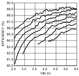
| L = 10 µH | 20 mA/String | ƒSW = 500 kHz |
| Top To Bottom: 2×4, 2×5, 2×6, 2×7, 2×8, 2×9 (LEDs) | ||
| L = 10 µH | 20 mA/String | ƒSW = 500 kHz |
| Top To Bottom: 1×4, 1×5, 1×6, 1×7, 1×8, 1×9, 1×10 (LEDs) | ||
| L = 4.7 µH | 20 mA/String | ƒSW = 1 MHz |
| Top To Bottom: 2×4, 2×5, 2×6, 2×7, 2×8, 2×9 (LEDs) | ||
| L = 22 µH | VIN = 3.6 V | ƒSW = 500 kHz |
| Top To Bottom: 1×4, 1×5, 1×6, 1×7, 1×8, 1×9, 1×10 (LEDs) | ||

| L = 10 µH | VIN = 3.6 V | ƒSW = 500 kHz |
| Top To Bottom: 2×4, 2×5, 2×6, 2×7, 2×8, 2×9, 2×10 (LEDs) | ||
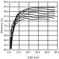
| L = 4.7 µH | VIN = 3.6 V | ƒSW = 1 MHz | ||
| Top To Bottom: 2×4, 2×5, 2×6, 2×7, 2×8, 2×9, 2×10 (LEDs) | ||||
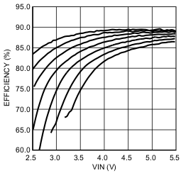
| L = 22 µH | 20 mA/String | ƒSW = 1 MHz |
| Top To Bottom: 2×4, 2×5, 2×6, 2×7, 2×8, 2×9, 2×10 (LEDs) | ||
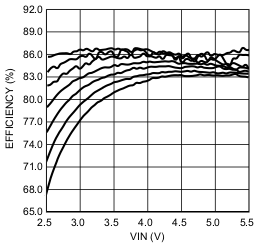
| L = 22 µH | 20 mA/String | ƒSW = 1 MHz |
| Top To Bottom: 1×4, 1×5, 1×6, 1×7, 1×8, 1×9, 1×10 (LEDs) | ||
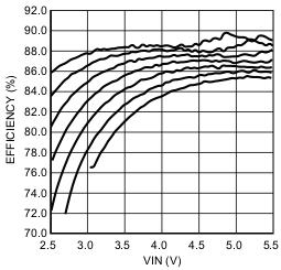
| L = 10 µH | 20 mA/String | ƒSW = 1 MHz |
| Top To Bottom: 2×4, 2×5, 2×6, 2×7, 2×8, 2×9, 2×10 (LEDs) | ||
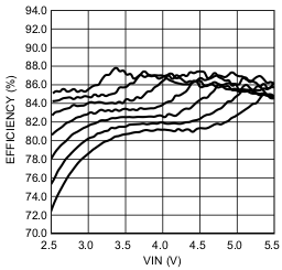
| L = 10 µH | 20 mA/String | ƒSW = 1 MHz |
| Top To Bottom: 1×4, 1×5, 1×6, 1×7, 1×8, 1×9, 1×10 (LEDs) | ||
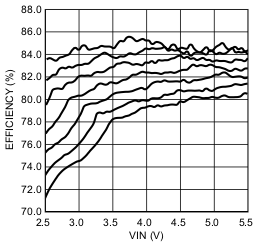
| L = 4.7 µH | 20 mA/String | |
| Top To Bottom: 1×4, 1×5, 1×6, 1×7, 1×8, 1×9, 1×10 (LEDs) | ||
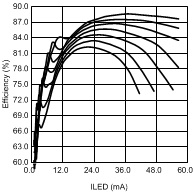
| L = 22 µH | VIN = 3.6 V | ƒSW = 1 MHz |
| Top To Bottom: 2×4, 2×5, 2×6, 2×7, 2×8, 2×9, 2×10 (LEDs) | ||
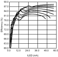
| L = 10 µH | VIN = 3.6 V | ƒSW = 1 MHz |
| Top To Bottom: 2×4, 2×5, 2×6, 2×7, 2×8, 2×9, 2×10 (LEDs) | ||