SNVS594G December 2008 – April 2016 LM3555
PRODUCTION DATA.
- 1 Features
- 2 Applications
- 3 Description
- 4 Revision History
- 5 Pin Configuration and Functions
- 6 Specifications
-
7 Detailed Description
- 7.1 Overview
- 7.2 Functional Block Diagram
- 7.3 Feature Description
- 7.4 Device Functional Modes
- 7.5 Programming
- 7.6 Register Maps
- 8 Application and Implementation
- 9 Power Supply Recommendations
- 10Layout
- 11Device and Documentation Support
- 12Mechanical, Packaging, and Orderable Information
6 Specifications
6.1 Absolute Maximum Ratings
over operating free-air temperature range (unless otherwise noted)(1)(2)(3)| MIN | MAX | UNIT | ||
|---|---|---|---|---|
| VIN | −0.3 | 6 | V | |
| TORCH, IND, STROBE, I2C/EN, SDA/EN2, SCL/EN1 | −0.3 | (VIN + 0.3 V) w/ 6 V maximum | V | |
| SW | 12 | V | ||
| VOUT, VLED | 10 | V | ||
| Continuous power dissipation(4) | Internally limited | |||
| Junction temperature, TJ-MAX | 150 | °C | ||
| Maximum lead temperature (soldering) | See(5) | |||
| Storage temperature, Tstg | –55 | 150 | °C | |
(1) Stresses beyond those listed under Absolute Maximum Ratings may cause permanent damage to the device. These are stress ratings only, which do not imply functional operation of the device at these or any other conditions beyond those indicated under Recommended Operating Conditions. Exposure to absolute-maximum-rated conditions for extended periods may affect device reliability.
(2) All voltages are with respect to the potential at the GND pin.
(3) If Military/Aerospace specified devices are required, contact the Texas Instruments Sales Office/ Distributors for availability and specifications.
(4) Internal thermal shutdown circuitry protects the device from permanent damage. Thermal shutdown engages at TJ=150°C (typical) and disengages at TJ=135°C (typical). Thermal shutdown is specified by design.
(5) For detailed soldering specifications and information, please refer to AN-1112 DSBGA Wafer Level Chip Scale Package (SNVA009).
6.2 ESD Ratings
| VALUE | UNIT | |||
|---|---|---|---|---|
| V(ESD) | Electrostatic discharge | Human-body model (HBM), per ANSI/ESDA/JEDEC JS-001(1) | ±2500 | V |
(1) JEDEC document JEP155 states that 500-V HBM allows safe manufacturing with a standard ESD control process.
6.3 Recommended Operating Conditions
over operating free-air temperature range (unless otherwise noted)(1)(2)| MIN | MAX | UNIT | ||
|---|---|---|---|---|
| Input voltage | 2.5 | 5.5 | V | |
| Junction temperature, TJ | −30 | 125 | °C | |
| Ambient temperature, TA(3) | −30 | 85 | °C | |
(1) Absolute Maximum Ratings indicate limits beyond which damage to the device may occur. Recommended Operating Ratings are conditions under which operation of the device is specified. Operating Ratings do not imply specified performance limits. For specified performance limits and associated test conditions, see the Electrical Characteristics tables.
(2) All voltages are with respect to the potential at the GND pin.
(3) In applications where high power dissipation and/or poor package thermal resistance is present, the maximum ambient temperature may have to be de-rated. Maximum ambient temperature (TA-MAX) is dependent on the maximum operating junction temperature (TJ-MAX-OP = 125°C), the maximum power dissipation of the device in the application (PD-MAX), and the junction-to-ambient thermal resistance of the part/package in the application (RθJA), as given by the following equation: TA-MAX = TJ-MAX-OP – (RθJA × PD-MAX).
6.4 Thermal Information
| THERMAL METRIC(1) | LM3555 | UNIT | |
|---|---|---|---|
| YZR (DSBGA) | |||
| 12 PINS | |||
| RθJA | Junction-to-ambient thermal resistance | 92.9 | °C/W |
| RθJC(top) | Junction-to-case (top) thermal resistance | 0.6 | °C/W |
| RθJB | Junction-to-board thermal resistance | 16.1 | °C/W |
| ψJT | Junction-to-top characterization parameter | 2.8 | °C/W |
| ψJB | Junction-to-board characterization parameter | 16.1 | °C/W |
(1) For more information about traditional and new thermal metrics, see the Semiconductor and IC Package Thermal Metrics application report, SPRA953.
6.5 Electrical Characteristics
Unless otherwise specified: typical limits are for TA = 25°C; minimum and maximum limits apply over the full operating ambient temperature range (−30°C ≤ TA ≤ +85°C); VIN = 3.6 V.(1)(2)| PARAMETER | TEST CONDITIONS | MIN | TYP | MAX | UNIT | ||
|---|---|---|---|---|---|---|---|
| CURRENT AND VOLTAGE SPECIFICATIONS | |||||||
| ILED-OUT | Flash LED accuracy | 2.7 V ≤ VIN ≤ 5.5 V VOUT = 6.5 V, VLED = 6.2 V |
50.7 (–15.5%) |
60 | 67.2 (12%) |
mA (%) | |
| 69.8 (–12.8%) |
80 | 86.4 (8%) |
|||||
| 304 (–5%) |
320 | 336 (5%) |
|||||
| 475 (–5%) |
500 | 535 (7%) |
|||||
| IIND-OUT | Indicator LED current accuracy | 2.7 V ≤ VIN ≤ 5.5 V, VIND = 2 V (indicator mode) | –20.4% | 2.5 mA | 33.6% | ||
| –20.4% | 5 mA | 33.8% | |||||
| –20.3% | 7.5 mA | 33.7% | |||||
| –20.2% | 10 mA | 33.4% | |||||
| VCSH | Current source headroom voltage | 2.7 V ≤ VIN ≤ 5.5 V | 300 | 350 | mV | ||
| VOVP | Overvoltage Protection Range | 2.7 V ≤ VIN ≤ 5.5 V | Trip point (rising) | 9.22 | 9.5 | 9.96 | V |
| Hysteresis | 0.4 | ||||||
| VOUT | Output voltage range | (VLED × NLED) + VCSH | Upper range | 8.5 | V | ||
| Lower range | 2.8 | ||||||
| ISD | Shutdown current | 2.7 V ≤ VIN ≤ 5.5 V | 0.75 | µA | |||
| ISB | Standby current | 2.7 V ≤ VIN ≤ 5.5 V | 1.1 | 4.3 | µA | ||
| IQ | Operating quiescent current | 2.7 V ≤ VIN ≤ 5.5 V, device switching | 3.5 | mA | |||
| VREF | Reference Voltage for LED Detection | VIN = 3.6 V (No Offset) | 4.35 | V | |||
| VIND | Indicator Fault Voltages | IND OVP | 2.571 | V | |||
| IND Short | 0.842 | ||||||
| UVLO | Undervoltage lockout | Falling VIN | 2.35 | 2.4 | 2.43 | V | |
| UVLOHYST | UVLO hysteresis | Rising VIN | 60 | 70 | 85 | mV | |
| ILIM | Peak current limit | 2.7 V ≤ VIN ≤ 5.5 V(3) | Current limit register value = 00 |
1.183 | 1.250 | 1.55 | A |
| Current limit register value = 01 |
1.417 | 1.500 | 1.781 | ||||
| Current limit register value = 10 |
1.512 | 1.750 | 2.025 | ||||
| Current limit register value = 11 |
1.805 | 2 | 2.267 | ||||
| OSCILLATOR AND TIMING SPECIFICATIONS (NON-I2C INTERFACE TIMING) | |||||||
| ƒSW | Switching frequency | 2.7 V ≤ VIN ≤ 5.5 V | 1.91 (−4.5%) |
2 | 2.15 (7.5%) |
MHz | |
| tHW | Hardware flash timeout | Default timer | 850 | msec | |||
| tRU | Current ramp-up time | ILED = 0mA to ILED = fullscale, VOUT = 6.5 V, VLED = 6.2 V |
0.6 | 1 | msec | ||
| tRD | Current ramp down time | ILED = fullscale to ILED = 0 mA VOUT = 6.5 V, VLED = 6.2 V |
0.2 | 0.5 | msec | ||
| tTORCH-DG | Torch deglitching time | 6.3 | 9 | 11.7 | msec | ||
| CONTROL INTERFACE VOLTAGE SPECIFICATIONS | |||||||
| VI2C/EN | I2C/EN pin voltage threshold | 2.7 V ≤ VIN ≤ 5.5 V | Simple mode | 0.54 | V | ||
| I2C mode | 1.26 | ||||||
| VIL | Low-level threshold voltage (SCL/EN1 and SDA/EN2) | 2.7 V ≤ VIN ≤ 5.5 V | 0.54 | V | |||
| VIH | High-level threshold voltage (SCL/EN1 and SDA/EN2) | 2.7 V ≤ VIN ≤ 5.5 V | 1.26 | V | |||
| VOL | Low-level output threshold limit (SDA/EN2) | ILOAD = 3 mA | 0.4 | V | |||
(1) Minimum (MIN) and maximum (MAX) limits are specified by design, test, or statistical analysis. Typical (TYP) numbers are not specified, but do represent the most likely norm. Unless otherwise specified, conditions for typical specifications are: VIN = 3.6 V and TA = 25°C.
(2) Switching disabled.
(3) TA (minimum) = 0°C to account for self-heating. Current Limit specification uses VIN (maximum) = 4 V to account for the input voltage range where current limit could be reached based upon the maximum application specifications for output voltage and diode current. Operation above 4 V and up to 5.5 V is allowed and must not reach current limit.
6.6 Control Interface Timing Requirements
| MIN | NOM | MAX | UNIT | ||
|---|---|---|---|---|---|
| TI2C-Start | I2C logic start-up time (I2C/EN going high) | 250 | 500 | µsec | |
| ƒSCL | SCL clock frequency | 400 | kHz | ||
| tI2C | I2C hang-up time | 35 | msec | ||
| tLOW | Low Period of SCL clock | 1.3 | µsec | ||
| tHIGH | High Period of SCL clock | 0.6 | µsec | ||
| tHD-STA | Hold Time (repeated) START condition | 0.6 | µsec | ||
| tSU-STA | Setup time for a repeated START condition | 0.6 | µsec | ||
| tHD-DAT | Data hold time | 0 | µsec | ||
| tSU-DAT | Data setup time | 100 | nsec | ||
| tR | Rise time for SCL and SDA | 300 | nsec | ||
| tF | Fall time for SCL and SDA | 300 | nsec | ||
| tSU-STO | Setup time for stop condition | 0.6 | µsec | ||
| tBUF | Bus free time between stop and start condition | 1.3 | µsec | ||
| tVD-DAT | Data valid time | 0.9 | µsec | ||
| tVD-ACK | Data valid acknowledge time | 0.9 | µsec | ||
| CB | Capacitive load for each bus line | 20 + 0.1 × CB | 400 | pF | |
6.7 Typical Characteristics
Unless otherwise specified: TA = 25°C; VIN = 3.6 V; CIN1= 10 µF, CIN2= 0.1 µF, COUT = 11 µF; L = 2.2 µH.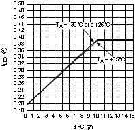
| Two Series LEDs Flash |

| Two series LEDs at 320 mA |

| Two Series LEDs at 400 mA |
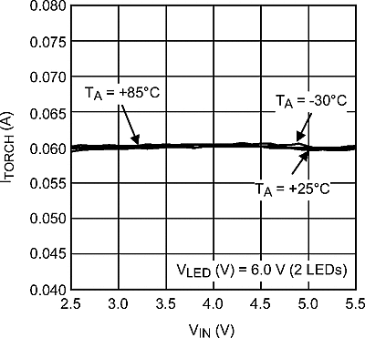
| Two LEDs at 60 mA |


| One LED at 500 mA |

| One LED at 60 mA |

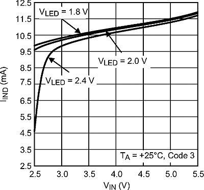


| Two LEDs | I2C Mode |

| Two LEDs | I2C Mode |

| Two LEDs | Simple Mode |


| Two Series LEDs at 320 mA |

| Two series LEDs at 400 mA |

| 2 LEDs |

| Two LEDs at 80 mA |

| One LED at 500 mA |
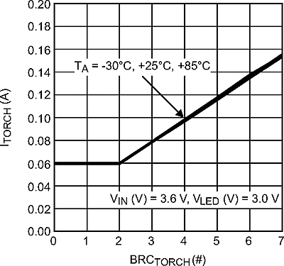
| One LED |

| One LED at 80 mA |
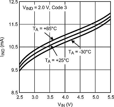
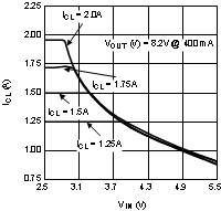


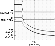
| Two LEDs | I2C Mode |

| Two LEDs | Simple Mode |

| Two LEDs | Torch |


