JAJSDP5D February   2016  – March 2018 LM36273

PRODUCTION DATA.  

  1. 特長
  2. アプリケーション
    1.     概略回路図
  3. 概要
    1.     バックライト効率、3P7S
  4. 改訂履歴
  5. Pin Configuration and Functions
    1.     Pin Functions
  6. Specifications
    1. 6.1 Absolute Maximum Ratings
    2. 6.2 ESD Ratings
    3. 6.3 Recommended Operating Conditions
    4. 6.4 Thermal Information
    5. 6.5 Electrical Characteristics
    6. 6.6 I2C Timing Requirements (Fast Mode)
    7. 6.7 Typical Characteristics
  7. Detailed Description
    1. 7.1 Overview
    2. 7.2 Functional Block Diagram
    3. 7.3 Features Description
      1. 7.3.1 Enabling the LM36273
      2. 7.3.2 Backlight
        1. 7.3.2.1 Current Sink Enable
        2. 7.3.2.2 Brightness Mapping
          1. 7.3.2.2.1 Linear Mapping
          2. 7.3.2.2.2 Exponential Mapping
        3. 7.3.2.3 Backlight Brightness Control Modes
          1. 7.3.2.3.1 I2C Brightness Control (PWM Pin Disabled)
          2. 7.3.2.3.2 I2C × PWM Brightness Control (PWM Pin Enabled)
            1. 7.3.2.3.2.1 PWM Ramper
        4. 7.3.2.4 Boost Switching Frequency
          1. 7.3.2.4.1 Minimum Inductor Select
        5. 7.3.2.5 Boost Feedback Gain Select
        6. 7.3.2.6 Auto Switching Frequency
        7. 7.3.2.7 PWM Input
          1. 7.3.2.7.1 PWM Sample Frequency
            1. 7.3.2.7.1.1 PWM Resolution and Input Frequency Range
            2. 7.3.2.7.1.2 PWM Sample Rate and Efficiency
              1. 7.3.2.7.1.2.1 PWM Sample Rate Example
          2. 7.3.2.7.2 PWM Hysteresis
          3. 7.3.2.7.3 PWM Step Response
          4. 7.3.2.7.4 PWM Timeout
          5. 7.3.2.7.5 PWM-to-Digital Code Readback
        8. 7.3.2.8 Regulated Headroom Voltage
        9. 7.3.2.9 Backlight Fault Protection and Faults
          1. 7.3.2.9.1 Backlight Overvoltage Protection (OVP)
          2. 7.3.2.9.2 Backlight Overcurrent Protection (OCP)
      3. 7.3.3 LCM Bias
        1. 7.3.3.1 Display Bias Boost Converter (VVPOS, VVNEG)
        2. 7.3.3.2 Auto Sequence Mode
        3. 7.3.3.3 Wake-up Mode
          1. 7.3.3.3.1 Wake1 Mode
          2. 7.3.3.3.2 Wake2 Mode
        4. 7.3.3.4 Active Discharge
        5. 7.3.3.5 LCM Bias Protection and Faults
          1. 7.3.3.5.1 LCM Overvoltage (OVP) Protection
          2. 7.3.3.5.2 VPOS Short-Circuit Protection
          3. 7.3.3.5.3 VNEG Short-Circuit Protection
      4. 7.3.4 Software Reset
      5. 7.3.5 HWEN Input
      6. 7.3.6 Thermal Shutdown (TSD)
    4. 7.4 Device Functional Modes
      1. 7.4.1 Modes of Operation
    5. 7.5 Programming
      1. 7.5.1 I2C-Compatible Serial Bus Interface
        1. 7.5.1.1 Interface Bus Overview
        2. 7.5.1.2 Data Transactions
        3. 7.5.1.3 Acknowledge Cycle
        4. 7.5.1.4 Acknowledge After Every Byte Rule
        5. 7.5.1.5 Addressing Transfer Formats
        6. 7.5.1.6 Register Programming
    6. 7.6 Register Maps
      1. 7.6.1  Revision Register (Address = 0x01)[Reset = 0x01]
        1. Table 11. Revision Register Field Descriptions
      2. 7.6.2  Backlight Configuration1 Register (Address = 0x02)[Reset = 0x28]
        1. Table 12. Backlight Configuration 1 Register Field Descriptions
      3. 7.6.3  Backlight Configuration 2 Register (Address = 0x03)[Reset = 0x8D]
        1. Table 13. Backlight Configuration 2 Register Field Descriptions
      4. 7.6.4  Backlight Brightness LSB Register (Address = 0x04)[Reset = 0x07]
        1. Table 14. Backlight Brightness LSB Register Field Descriptions
      5. 7.6.5  Backlight Brightness MSB Register (Address = 0x05)[Reset = 0xFF]
        1. Table 15. Backlight Brightness MSB Register Field Descriptions
      6. 7.6.6  Backlight Auto-Frequency Low Threshold Register (Address = 0x06)[Reset = 0x00]
        1. Table 16. Backlight Auto-Frequency Low Threshold Field Descriptions
      7. 7.6.7  Backlight Auto-Frequency High Threshold Register (Address = 0x07)[Reset = 0x00]
        1. Table 17. Backlight Auto-Frequency High Threshold Field Descriptions
      8. 7.6.8  Backlight Enable Register (Address = 0x08)[Reset = 0x00]
        1. Table 18. Backlight Enable Register Field Descriptions
      9. 7.6.9  Bias Configuration 1 Register (Address = 0x09)[Reset = 0x18]
        1. Table 19. Bias Configuration 1 Register Field Descriptions
      10. 7.6.10 Bias Configuration 2 register (Address = 0x0A)[Reset = 0x11]
        1. Table 20. Bias Configuration 2 Register Field Descriptions
      11. 7.6.11 Bias Configuration 3 Register (Address = 0x0B)[Reset = 0x00]
        1. Table 21. Bias Configuration 3 Register Field Descriptions
      12. 7.6.12 LCM Boost Bias Register (Address = 0x0C)[Reset = 0x28]
        1. Table 22. LCM Boost Bias Register Field Descriptions
      13. 7.6.13 VPOS Bias Register (Address = 0x0D)[Reset = 0x1E]
        1. Table 23. VPOS Bias Register Field Descriptions
      14. 7.6.14 VNEG Bias Register (Address = 0x0E)[Reset = 0x1C]
        1. Table 24. VNEG Bias Register Field Descriptions
      15. 7.6.15 Flags Register (Address = 0x0F)[Reset = 0x00]
        1. Table 25. Flags Register Field Descriptions
      16. 7.6.16 Option 1 Register (Address = 0x10)[Reset = 0x06]
        1. Table 26. Option 1 Register Field Descriptions
      17. 7.6.17 Option 2 Register (Address = 0x11)[Reset = 0x35]
        1. Table 27. Option 2 Register Field Descriptions
      18. 7.6.18 PWM-to-Digital Code Readback LSB Register (Address = 0x12)[Reset = 0x00]
        1. Table 28. PWM-to-Digital Code Readback LSB Register Field Descriptions
      19. 7.6.19 PWM-to-Digital Code Readback MSB Register (Address = 0x13)[Reset = 0x00]
        1. Table 29. PWM-to-Digital Code Readback MSB Register Field Descriptions
  8. Application and Implementation
    1. 8.1 Application Information
    2. 8.2 Typical Application
      1. 8.2.1 Design Requirements
      2. 8.2.2 Detailed Design Procedure
        1. 8.2.2.1 Component Selection
          1. 8.2.2.1.1 Inductor Selection
          2. 8.2.2.1.2 Boost Output Capacitor Selection
          3. 8.2.2.1.3 Input Capacitor Selection
      3. 8.2.3 Application Curves
        1. 8.2.3.1 Backlight Curves
          1. 8.2.3.1.1 Two LED Strings
          2. 8.2.3.1.2 Three LED Strings
        2. 8.2.3.2 LCM Bias Curves
  9. Power Supply Recommendations
  10. 10Layout
    1. 10.1 Layout Guidelines
    2. 10.2 Layout Example
  11. 11デバイスおよびドキュメントのサポート
    1. 11.1 デバイス・サポート
      1. 11.1.1 デベロッパー・ネットワークの製品に関する免責事項
      2. 11.1.2 開発サポート
    2. 11.2 ドキュメントのサポート
      1. 11.2.1 関連資料
    3. 11.3 ドキュメントの更新通知を受け取る方法
    4. 11.4 コミュニティ・リソース
    5. 11.5 商標
    6. 11.6 静電気放電に関する注意事項
    7. 11.7 Glossary
  12. 12メカニカル、パッケージ、および注文情報

パッケージ・オプション

メカニカル・データ(パッケージ|ピン)
サーマルパッド・メカニカル・データ
発注情報

Pin Configuration and Functions

YFF Package
24-Pin DSBGA
Top View
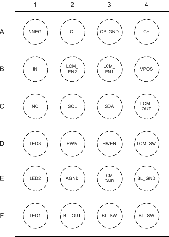
LM36273 LM36273_pin_diag.gif

Pin Functions

PIN TYPE DESCRIPTION
NUMBER NAME
A1 VNEG O Inverting charge pump output. Bypass VNEG with a 10-µF ceramic capacitor to CP_GND.
A2 C- O Inverting charge-pump flying capacitor negative connection
A3 CP_GND Charge pump GND. Connect the CNEG capacitor negative terminal to this pin.
A4 C+ O Inverting charge-pump flying capacitor positive connection
B1 IN I Input voltage connection. Bypass IN with a 10-µF ceramic capacitor to GND.
B2 LCM_EN2 I Enable for LCD bias negative output; 300-kΩ internal pulldown resistor between LCM_EN2 and GND.
B3 LCM_EN1 I Enable for LCD bias positive output; 300-kΩ internal pulldown resistor between LCM_EN1 and GND.
B4 VPOS O Positive LCD bias output. Bypass VPOS with a 10-µF ceramic capacitor to GND.
C1 NC No connect; leave this pin disconnected
C2 SCL I Serial clock connection for I2C-compatible interface
C3 SDA I/O Serial clock connection for I2C-compatible interface
C4 LCM_OUT O LCD bias boost output voltage. Bypass LCM_OUT with a 10-µF ceramic capacitor to LCM_GND.
D1 LED3 I Current sink 3 input. Connect the cathode of LED string 3 to this pin. Leave this pin disconnected if not used.
D2 PWM I PWM input for duty cycle current control; 300-kΩ internal pulldown resistor between PWM and GND.
D3 HWEN I Active high chip enable; 300-kΩ internal pulldown resistor between HWEN and GND.
D4 LCM_SW O LCD bias boost inductor connection
E1 LED2 I Current sink 2 input. Connect the cathode of LED string 2 to this pin. Leave this pin disconnected if not used.
E2 AGND Analog ground connection. Connect AGND directly to GND on the PCB.
E3 LCM_GND LCD bias boost GND connection. Connect LCM_GND to the negative terminal of the LCD bias output capacitor.
E4 BL_GND Backlight boost output capacitor GND connection
F1 LED1 I Current sink 1 input. Connect the cathode of LED string 1 to this pin. Leave this pin disconnected if not used.
F2 BL_OUT O Backlight boost output voltage sense connection. Connect to the positive terminal of backlight boost output capacitor.
F3 BL_SW O Backlight boost inductor connection
F4 BL_SW O Backlight boost inductor connection