SNVSA63A April 2015 – September 2015 LM3632A
PRODUCTION DATA.
- 1 Features
- 2 Applications
- 3 Description
- 4 Revision History
- 5 Pin Configuration and Functions
- 6 Specifications
-
7 Detailed Description
- 7.1 Overview
- 7.2 Functional Block Diagram
- 7.3
Features Description
- 7.3.1 Backlight
- 7.3.2 LCM Bias
- 7.3.3 Flash
- 7.3.4 Software RESET
- 7.3.5 EN Input
- 7.3.6 Thermal Shutdown (TSD)
- 7.4 Device Functional Modes
- 7.5 Programming
- 7.6
Register Maps
- 7.6.1 Revision (Address = 0x01) [reset = 0x09]
- 7.6.2 Backlight Configuration1 (Address = 0x02) [reset = 0x30]
- 7.6.3 Backlight Configuration2 (Address = 0x03) [reset = 0x0D]
- 7.6.4 Backlight Brightness LSB (Address = 0x04) [reset = 0x07]
- 7.6.5 Backlight Brightness MSB (Address = 0x05) [reset = 0xFF]
- 7.6.6 Flash/Torch Current (Address = 0x06) [reset = 0x3E]
- 7.6.7 Flash Configuration (Address = 0x07) [reset = 0x2F]
- 7.6.8 VIN Monitor (Address = 0x08) [reset = 0x03]
- 7.6.9 I/O Control (Address = 0x09) [reset = 0x00]
- 7.6.10 Enable (Address = 0x0A) [reset = 0x00]
- 7.6.11 Flags1 (Address = 0x0B) [reset = 0x00]
- 7.6.12 Display Bias Configuration (Address = 0x0C) [reset = 0x18]
- 7.6.13 LCM Boost Bias (Address = 0x0D) [reset = 0x1E]
- 7.6.14 VPOS Bias (Address = 0x0E) [reset = 0x1E]
- 7.6.15 VNEG Bias (Address = 0x0F) [reset = 0x1C]
- 7.6.16 Flags2 (Address = 0x10) [reset = 0x00]
- 8 Application and Implementation
- 9 Power Supply Recommendations
- 10Layout
- 11Device and Documentation Support
- 12Mechanical, Packaging, and Orderable Information
8 Application and Implementation
NOTE
Information in the following applications sections is not part of the TI component specification, and TI does not warrant its accuracy or completeness. TI’s customers are responsible for determining suitability of components for their purposes. Customers should validate and test their design implementation to confirm system functionality.
8.1 Application Information
The LM3632A integrates an LCD backlight driver, LCM positive and negative bias voltage supplies, and a flash driver into a single device. The backlight boost converter generates the high voltage required for the LEDs. The device can drive one or two LED strings with 4 to 8 white LEDs per string. Positive and negative bias voltages are post-regulated from the LCM bias boost output voltage. The flash driver can supply constant current of up to a 1.5 A to the LED output. All three functions are independent of each other and can be enabled using their own dedicated controls.
8.2 Typical Application
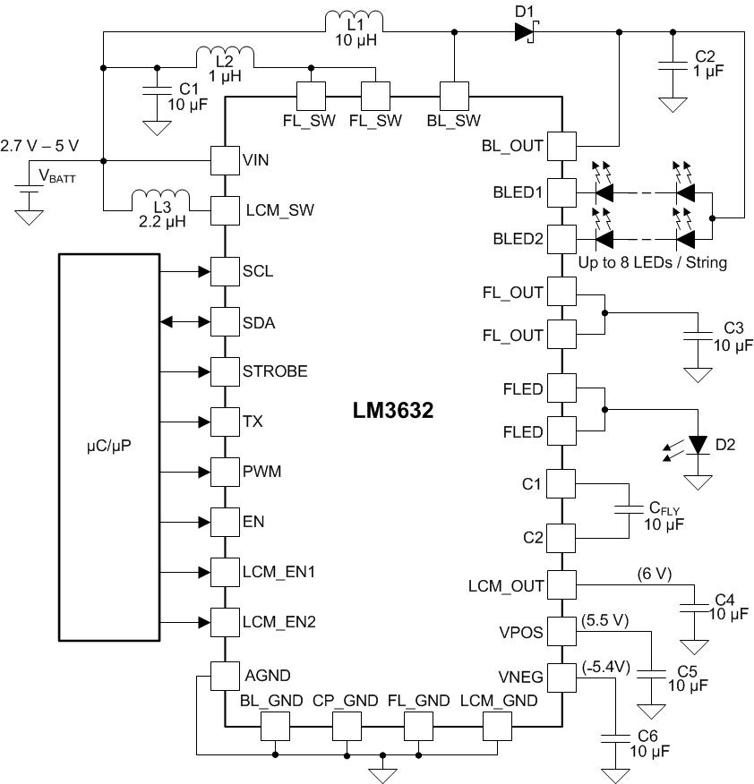 Figure 55. Typical Application Schematic
8.2.1 Design Requirements
Example requirements are shown below:
| DESIGN PARAMETER | EXAMPLE VALUE |
|---|---|
| Input voltage range | 2.7 V to 4.5 V (single Li-Ion cell battery) |
| Brightness control | I2C Register |
| Backlight LED configuration | 2 parallel, 6 series |
| Backlight LED current | max 25 mA / string |
| Backlight boost maximum voltage | 29 V |
| Backlight boost SW frequency | 1 MHz |
| Backlight boost inductor | 10 µH, 1-A saturation current |
| LCM boost output voltage | 6 V |
| VVNEG output voltage | –5.4 V |
| VVPOS output voltage | 5.5 V |
| Flash LED current | 1.5 A |
| Torch LED current | 100 mA |
8.2.2 Detailed Design Procedure
8.2.2.1 External Components
Table 23 shows examples of external components for the LM3632A. Boost converter output capacitors can be replaced with dual output capacitors of lower capacitance as long as the minimum effective capacitance requirement is met. DC bias effect of the ceramic capacitors must be taken into consideration when choosing the output capacitors. This is especially true for the high output-voltage backlight-boost converter.
Table 23. Recommended External Components
| DESIGNATOR (Figure 55) | DESCRIPTION | VALUE | EXAMPLE |
|---|---|---|---|
| C1, C3, C4, C5, C6 | Ceramic capacitor | 10 µF, 10 V | C1608X5R0J106M |
| C2 | Ceramic capacitor | 1 µF, 35 V | C2012X7R1H105K125AB |
| L1 | Inductor | 10 µH, 1 A | VLF403212MT- 100M |
| L2 | Inductor | 1 µH, 2.8 A | DFE201610P-1R0M |
| L3 | Inductor | 2.2 µH, 1 A | VLS201612ET-2R2M |
| D1 | Schottky diode | 30 V, 500 mA | NSR0530P2T5G |
8.2.2.2 Inductor Selection
Both of the LM3632A boost converters are internally compensated. The compensation parameters are designed for the inductance values listed on Table 23. Effective inductance of the inductors should be ±20%.
There are two main considerations when choosing an inductor: the inductor should not saturate, and the inductor current ripple should be small enough to achieve the desired output voltage ripple. Different saturation current rating specifications are followed by different manufacturers so attention must be given to details. Saturation current ratings are typically specified at 25°C. However, ratings at the maximum ambient temperature of the application should be requested from the manufacturer. The saturation current should be greater than the sum of the maximum load current and the worst-case average-to-peak inductor current. When the boost device is boosting (VOUT > VIN) the inductor is one of the largest area of efficiency loss in the circuit. Therefore, choosing an inductor with the lowest possible series resistance is important, especially for the flash and LCM Bias converters. For proper inductor operation and circuit performance, ensure that the inductor saturation and the peak current limit setting of the LM3632A are greater than IPEAK in Equation 5:

See detailed information in “Understanding Boost Power Stages in Switch Mode Power Supplies” http://focus.ti.com/lit/an/slva061/slva061.pdf. “Power Stage Designer™ Tools” can be used for the boost calculation: http://www.ti.com/tool/powerstage-designer.
8.2.2.3 Boost Output Capacitor Selection
At least an 1-μF capacitor is recommended for the backlight boost converter output capacitor. A high-quality ceramic type X5R or X7R is recommended. Voltage rating must be greater than the maximum output voltage that is used. The effective output capacitance should always remain higher than 0.4 µF for stable operation.
For the LCM bias boost output a high-quality 10-μF ceramic type X5R or X7R capacitor is recommended. Voltage rating must be greater than the maximum output voltage that is used.
The flash driver is designed to operate with a 10-μF ceramic output capacitor. When the boost converter is running, the output capacitor supplies the load current during the boost converter's on-time. When the NMOS switch turns off, the inductor energy is discharged through the internal PMOS switch, supplying power to the load and restoring charge to the output capacitor. This causes a sag in the output voltage during the on-time and a rise in the output voltage during the off-time. The output capacitor is therefore chosen to limit the output ripple to an acceptable level depending on load current and input/output voltage differentials and also to ensure the converter remains stable.
The DC-bias effect of the capacitors must be taken into consideration when selecting the output capacitors. The effective capacitance of a ceramic capacitor can drop down to less than 10% with maximum rated DC bias voltage. Note that with a same voltage applied, the capacitors with higher voltage rating suffer less from the DC-bias effect than capacitors with lower voltage rating.
8.2.2.4 Input Capacitor Selection
Choosing the correct size and type of input capacitor helps minimize the voltage ripple caused by the switching of the LM3632A boost converters and reduce noise on the boost converter's input pin that can feed through and disrupt internal analog signals. In Figure 55 a 10-μF ceramic input capacitor works well. It is important to place the input capacitor as close as possible to the LM3632A input (VIN) pin. This reduces the series resistance and inductance that can inject noise into the device due to the input switching currents.
8.2.3 Application Curves
8.2.3.1 Backlight Curves
Ambient temperature is 25°C and VIN is 3.7 V unless otherwise noted. Backlight System Efficiency is defined as PLED / PIN, where PLED is actual power consumed in backlight LEDs.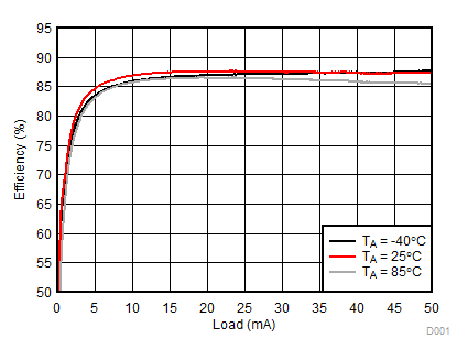
| 2p7s LEDs | ƒ = 500 kHz |

| 2p7s LEDs | ƒ = 1 MHz |
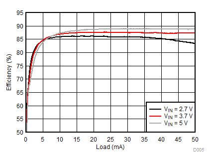
| 2p7s LEDs | ƒ = 500 kHz |
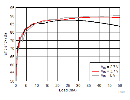
| 2p7s LEDs | ƒ = 1 MHz |
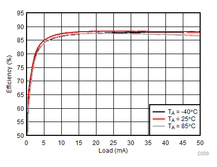
| 2p6s LEDs | ƒ = 500 kHz |
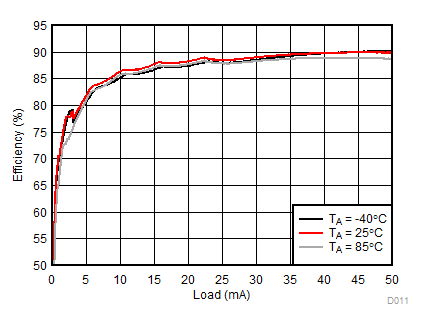
| 2p6s LEDs | ƒ = 1 MHz |
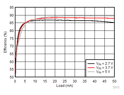
| 2p6s LEDs | ƒ = 500 kHz |
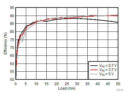
| 2p6s LEDs | ƒ = 1 MHz |
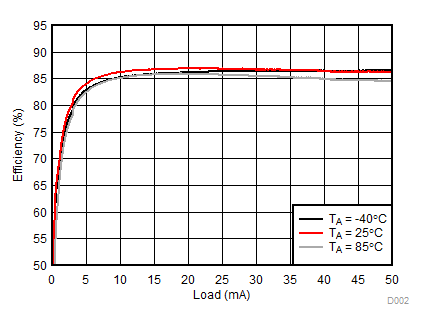
| 2p7s LEDs | ƒ = 500 kHz |
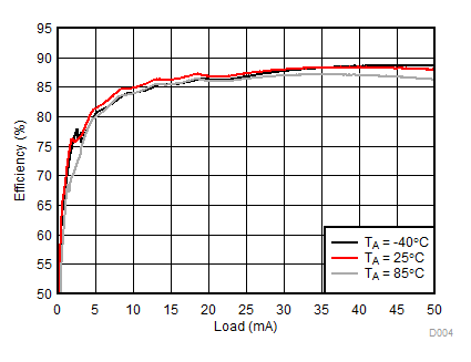
| 2p7s LEDs | ƒ = 1 MHz |
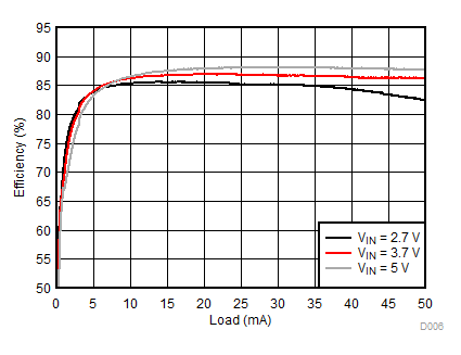
| 2p7s LEDs | ƒ = 500 kHz |
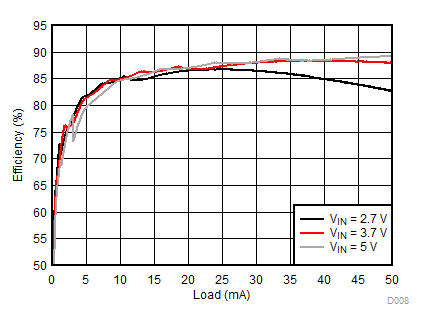
| 2p7s LEDs | ƒ = 1 MHz |
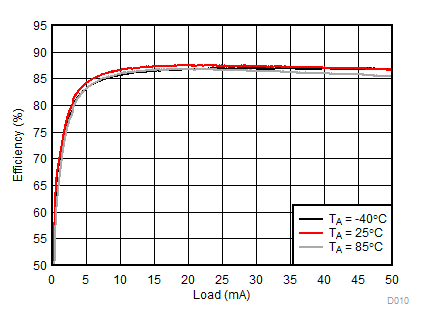
| 2p6s LEDs | ƒ = 500 kHz |
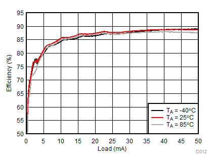
| 2p6s LEDs | ƒ = 1 MHz |
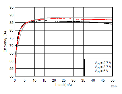
| 2p6s LEDs | ƒ = 500 kHz |
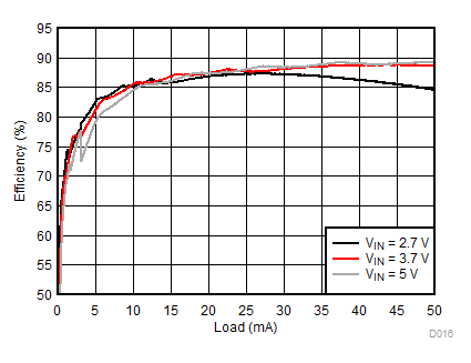
| 2p6s LEDs | ƒ = 1 MHz |
8.2.3.2 LCM Bias Curves
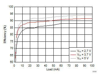
Ambient temperature is 25°C and VIN is 3.7 V unless otherwise noted. VPOS, VNEG and VPOS/VNEG Efficiency is defined as POUT / PIN, where POUT is actual power consumed in VPOS, VNEG and (VPOS + VNEG) outputs, respectively.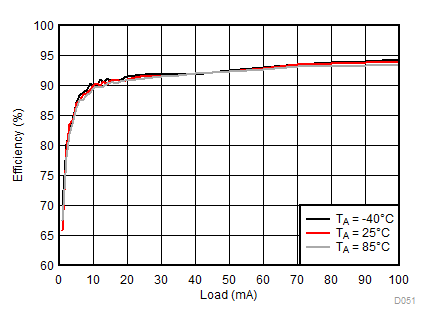
| VLCM_OUT = 4.5 V |
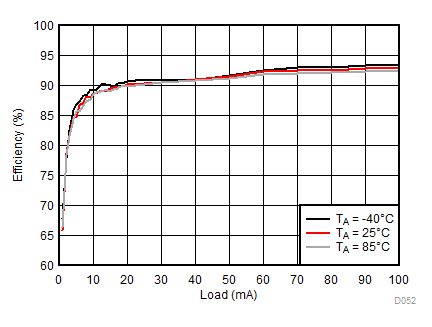
| VLCM_OUT = 5 V |
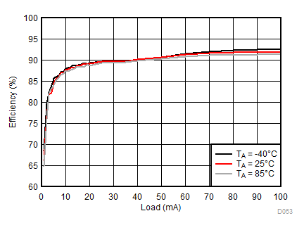
| VLCM_OUT = 5.5 V |
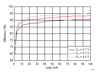
| VLCM_OUT = 4.8 V |
| VLCM_OUT = 5.9 V |
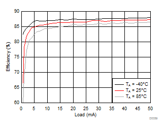
| VVPOS = 5 V | VLCM_OUT = 5.4 V |
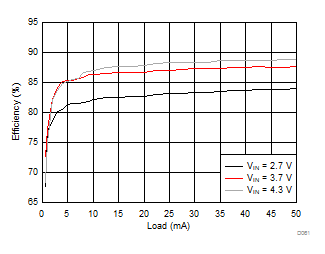
| VVPOS = 4.5 V | VLCM_OUT = 4.9 V | |
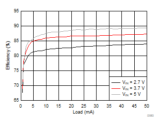
| VVPOS = 5.5 V | VLCM_OUT = 5.9 V |
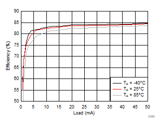
| VVNEG = –5 V | VLCM_OUT = 5.4 V |
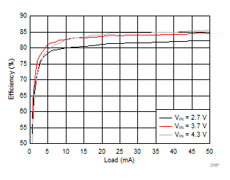
| VVNEG = –4.5 V | VLCM_OUT = 4.9 V |
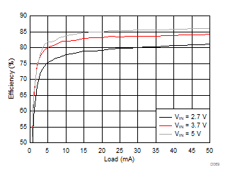
| VVNEG = –5.5 V | VLCM_OUT = 5.9 V |
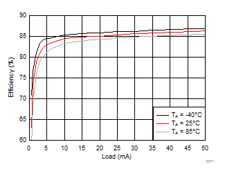
| VVPOS = 5 V | VVNEG = –5 V | VLCM_OUT = 5.4 V |
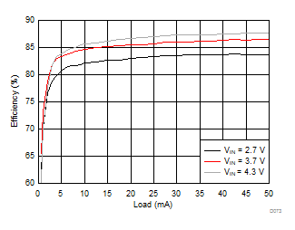
| VVPOS = 4.5 V | VVNEG = –4.5 V | VLCM_OUT = 4.9 V |
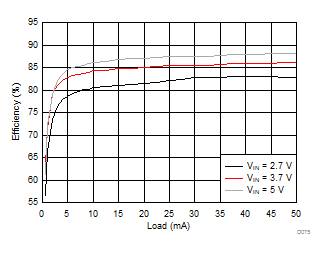
| VVPOS = 5.5 V | VVNEG = –5.5 V | VLCM_OUT = 5.9 V |
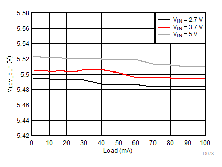
| VLCM_OUT = 5.5 V |
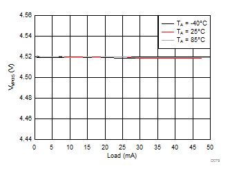
| VVPOS = 4.5 V | VLCM_OUT = 4.9 V |
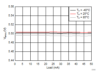
| VVPOS = 5.5 V | VLCM_OUT = 5.9 V |
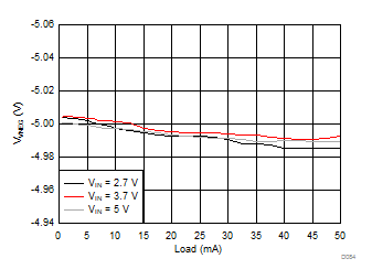
| VVNEG = –5 V | VLCM_OUT = 5.4 V |
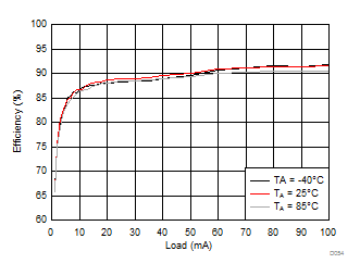
| VLCM_OUT = 6 V |
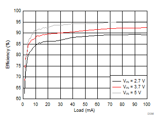
| VLCM_OUT = 5.3 V |
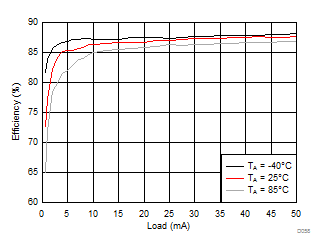
| VVPOS = 4.5 V | VLCM_OUT = 4.9 V |
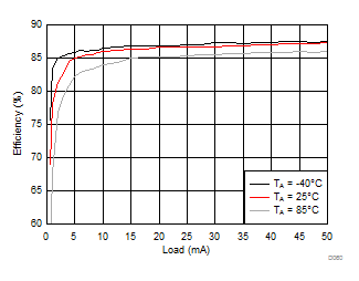
| VVPOS = 5.5 V | VLCM_OUT = 5.9 V | |
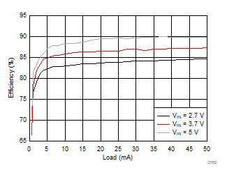
| VVPOS = 5 V | VLCM_OUT = 5.4 V |
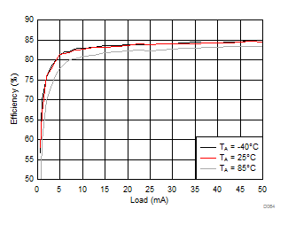
| VVNEG = –4.5 V | VLCM_OUT = 4.9 V |
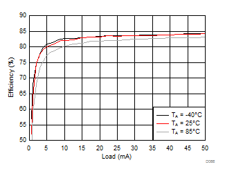
| VVNEG = –5.5 V | VLCM_OUT = 5.9 V | |
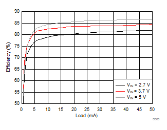
| VVNEG = –5 V | VLCM_OUT = 5.4 V |
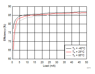
| VVPOS = 4.5 V | VVNEG = –4.5 V | VLCM_OUT = 4.9 V |
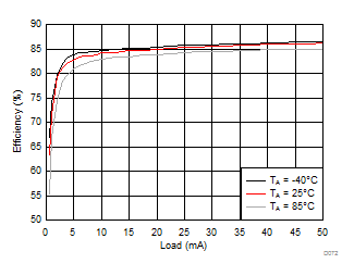
| VVPOS= 5.5 V | VVNEG = –5.5 V | VLCM_OUT = 5.9 V |
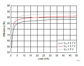
| VVPOS = 5 V | VVNEG = –5 V | VLCM_OUT = 5.4 V |
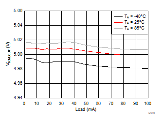
| VLCM_OUT = 5 V |
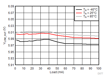
| VLCM_OUT = 6 V |
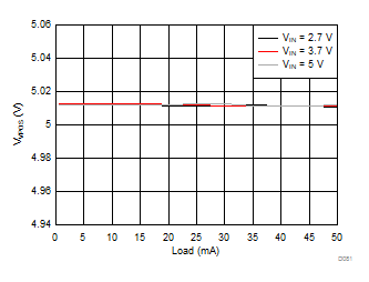
| VVPOS = 5 V | VLCM_OUT = 5.4 V |
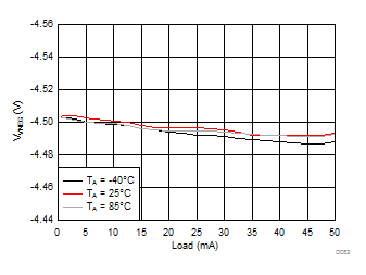
| VVNEG = –4.5 V | VLCM_OUT = 4.9 V |
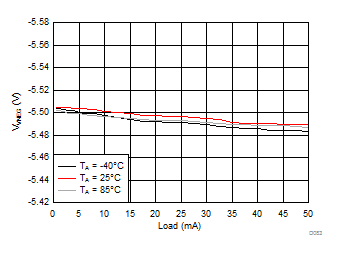
| VVNEG = –5.5 V | VLCM_OUT = 5.9 V |
8.2.3.3 Flash Curves
Ambient temperature is 25°C and VIN is 3.7 V unless otherwise noted. Flash System Efficiency defined as PLED / PIN, where PLED is actual power consumed in flash LED.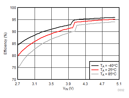
| IFLED = 1.5 A | ƒ = 4 MHz | VFLED = 3.5 V |
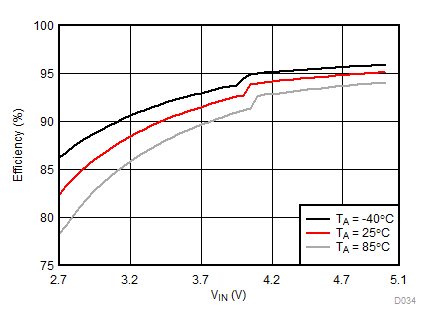
| IFLED = 1.5 A | ƒ = 2 MHz | VFLED = 3.5 V |
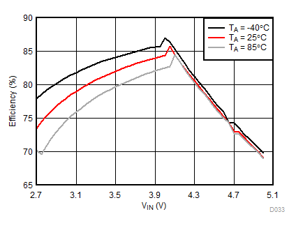
| IFLED = 1.5 A | ƒ = 4 MHz | VFLED = 3.5 V |
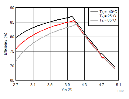
| IFLED = 1.5 A | ƒ = 2 MHz | VFLED = 3.5 V |
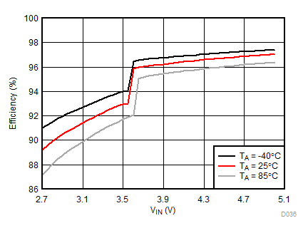
| IFLED = 0.8 A | ƒ = 4 MHz | VFLED = 3.2 V |
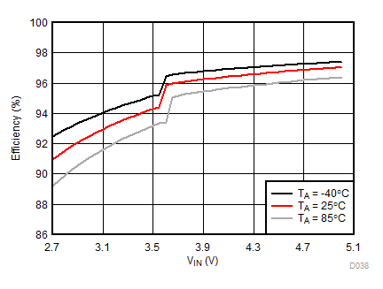
| IFLED = 0.8 A | ƒ = 2 MHz | VFLED = 3.2 V |
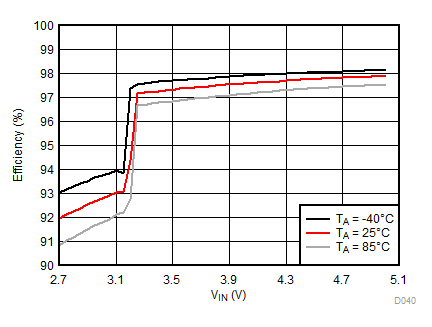
| IFLED = 375 mA | ƒ = 4 MHz | VFLED = 3 V |
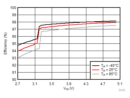
| IFLED = 375 mA | ƒ = 4 MHz | VFLED = 3 V |
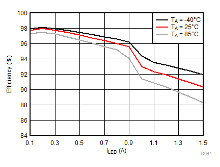
| ƒ = 4 MHz |
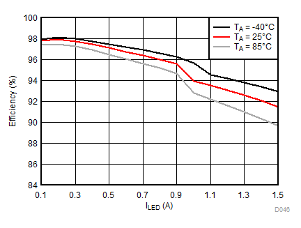
| ƒ = 2 MHz |
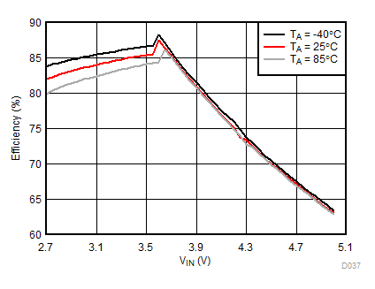
| IFLED = 0.8 A | ƒ = 4 MHz | VFLED = 3.2 V |
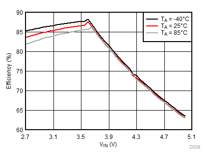
| IFLED = 0.8 A | ƒ = 2 MHz | VFLED = 3.2 V |
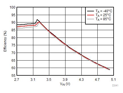
| IFLED = 375 mA | ƒ = 4 MHz | VFLED = 3 V |
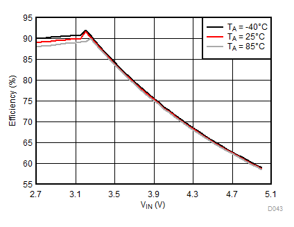
| IFLED = 375 mA | ƒ = 2 MHz | VFLED = 3 V |
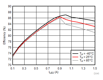
| ƒ = 4 MHz |
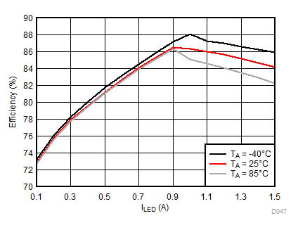
| ƒ = 2 MHz |