SNVSA63A April 2015 – September 2015 LM3632A
PRODUCTION DATA.
- 1 Features
- 2 Applications
- 3 Description
- 4 Revision History
- 5 Pin Configuration and Functions
- 6 Specifications
-
7 Detailed Description
- 7.1 Overview
- 7.2 Functional Block Diagram
- 7.3
Features Description
- 7.3.1 Backlight
- 7.3.2 LCM Bias
- 7.3.3 Flash
- 7.3.4 Software RESET
- 7.3.5 EN Input
- 7.3.6 Thermal Shutdown (TSD)
- 7.4 Device Functional Modes
- 7.5 Programming
- 7.6
Register Maps
- 7.6.1 Revision (Address = 0x01) [reset = 0x09]
- 7.6.2 Backlight Configuration1 (Address = 0x02) [reset = 0x30]
- 7.6.3 Backlight Configuration2 (Address = 0x03) [reset = 0x0D]
- 7.6.4 Backlight Brightness LSB (Address = 0x04) [reset = 0x07]
- 7.6.5 Backlight Brightness MSB (Address = 0x05) [reset = 0xFF]
- 7.6.6 Flash/Torch Current (Address = 0x06) [reset = 0x3E]
- 7.6.7 Flash Configuration (Address = 0x07) [reset = 0x2F]
- 7.6.8 VIN Monitor (Address = 0x08) [reset = 0x03]
- 7.6.9 I/O Control (Address = 0x09) [reset = 0x00]
- 7.6.10 Enable (Address = 0x0A) [reset = 0x00]
- 7.6.11 Flags1 (Address = 0x0B) [reset = 0x00]
- 7.6.12 Display Bias Configuration (Address = 0x0C) [reset = 0x18]
- 7.6.13 LCM Boost Bias (Address = 0x0D) [reset = 0x1E]
- 7.6.14 VPOS Bias (Address = 0x0E) [reset = 0x1E]
- 7.6.15 VNEG Bias (Address = 0x0F) [reset = 0x1C]
- 7.6.16 Flags2 (Address = 0x10) [reset = 0x00]
- 8 Application and Implementation
- 9 Power Supply Recommendations
- 10Layout
- 11Device and Documentation Support
- 12Mechanical, Packaging, and Orderable Information
10 Layout
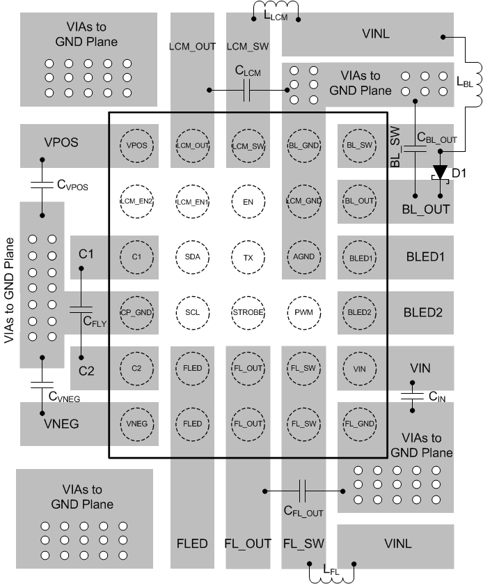
10.1 Layout Guidelines
- Place the boost converters output capacitors as close to the output voltage and GND pins as possible.
- Minimize the boost converter switching loops by placing the input capacitors and inductors close to GND and switch pins.
- If possible, route the switching loops on top layer only. For best efficiency, try to minimize copper on the switch node to minimize switch pin parasitic capacitance while preserving adequate routing width.
- VIN input voltage pin needs to be bypassed to ground with a low-ESR bypass capacitor. Place the capacitor as close to VIN pin as possible.
- Place the output capacitor of the LDO as close to the output pins as possible. Also place the charge pump flying capacitor and output capacitor close to their respective pins.
- Terminate the Flash LED cathode directly to the Flash GND pin of the LM3632A. If possible, route the LED return with a dedicated path so as to keep the high amplitude LED current out of the GND plane.
- Route the internal pins on the second layer. Use offset micro vias to go from top layer to mid-layer1. Avoid routing the signal traces directly under the switching loops of the boost converters.
10.2 Layout Example
