SNVSCV4 September 2024 LM3645
PRODUCTION DATA
- 1
- 1 Features
- 2 Applications
- 3 Description
- 4 Pin Configuration and Functions
- 5 Specifications
-
6 Detailed Description
- 6.1 Overview
- 6.2 Functional Block Diagram
- 6.3
Feature Description
- 6.3.1 Power Amplifier Synchronization (TORCH/TX)
- 6.3.2 Input Voltage Flash Monitor (IVFM)
- 6.3.3
Fault/Protections
- 6.3.3.1 Fault Operation
- 6.3.3.2 Flash Time-Out
- 6.3.3.3 Overvoltage Protection (OVP)
- 6.3.3.4 Current Limit
- 6.3.3.5 NTC Thermistor Input/Outputs (TEMP1, TEMP2)
- 6.3.3.6 Thermal Scale Back
- 6.3.3.7 Thermal Shutdown (TSD)
- 6.3.3.8 Undervoltage Lockout (UVLO)
- 6.3.3.9 LED and/or VOUT Short Fault
- 6.3.3.10 Fault Behavior Table
- 6.4 Device Functioning Modes
- 6.5 Programming and Control
- 6.6 Register Descriptions
- 7 Application and Implementation
- 8 Power Supply Recommendations
- 9 Layout
- 10Device and Documentation Support
- 11Revision History
- 12Mechanical, Packaging, and Orderable Information
4 Pin Configuration and Functions
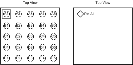
 Figure 4-1 YCG Package, 25-Pin DSBGA
Table 4-1 Pin Functions
| PIN | TYPE | DESCRIPTION | |
|---|---|---|---|
| NO. | NAME | ||
| A3 | IN | P | Input voltage connection. Connect this pin to the input supply and bypass to GND with a 10-µF or larger ceramic capacitor |
| B1 | SW | P | Drain connection for internal N-channel MOSFET and synchronous P-channel MOSFET switches |
| B2 | |||
| C1 | OUT | P | Step-up DC-DC converter output. Connect 2 × 10-µF ceramic capacitors between this terminal and GND |
| C2 | |||
| C3 | |||
| C4 | |||
| A1 | GND | G | Ground |
| A2 | |||
| E1 | D1 | P | High-side current source outputs for flash LEDs |
| E2 | |||
| D1 | D2 | P | |
| D2 | |||
| D4 | D3 | P | |
| D5 | |||
| E4 | D4 | P | |
| E5 | |||
| A4 | EN | I | Active high hardware enable. Drive EN pin high to turn on the device. An internal pulldown resistor of 300 kΩ is between EN and GND. |
| A5 | SDA | I/O | I2C serial data input/output |
| B5 | SCL | I | I2C serial clock input |
| B3 | STR1 | I | Active high hardware flash enable. Drive STR1 high to turn on flash or IR pulse. An internal pulldown resistor of 300 kΩ is between STR1 and GND. |
| B4 | STR2 | I | Active high hardware flash enable. Drive STR2 high to turn on flash or IR pulse. An internal pulldown resistor of 300 kΩ is between STR2 and GND. |
| C5 | TORCH/TX | I | Active high hardware torch enable or power amplifier synchronization input. Internal pulldown resistor of 300 kΩ between TORCH/TX and GND. |
| E3 | TEMP1 | I/O | Threshold detector for NTC temperature sensing and current scale back |
| D3 | TEMP2 | I/O | |