SNVSCV4 September 2024 LM3645
PRODUCTION DATA
- 1
- 1 Features
- 2 Applications
- 3 Description
- 4 Pin Configuration and Functions
- 5 Specifications
-
6 Detailed Description
- 6.1 Overview
- 6.2 Functional Block Diagram
- 6.3
Feature Description
- 6.3.1 Power Amplifier Synchronization (TORCH/TX)
- 6.3.2 Input Voltage Flash Monitor (IVFM)
- 6.3.3
Fault/Protections
- 6.3.3.1 Fault Operation
- 6.3.3.2 Flash Time-Out
- 6.3.3.3 Overvoltage Protection (OVP)
- 6.3.3.4 Current Limit
- 6.3.3.5 NTC Thermistor Input/Outputs (TEMP1, TEMP2)
- 6.3.3.6 Thermal Scale Back
- 6.3.3.7 Thermal Shutdown (TSD)
- 6.3.3.8 Undervoltage Lockout (UVLO)
- 6.3.3.9 LED and/or VOUT Short Fault
- 6.3.3.10 Fault Behavior Table
- 6.4 Device Functioning Modes
- 6.5 Programming and Control
- 6.6 Register Descriptions
- 7 Application and Implementation
- 8 Power Supply Recommendations
- 9 Layout
- 10Device and Documentation Support
- 11Revision History
- 12Mechanical, Packaging, and Orderable Information
6.5.5.3 Transferring Data
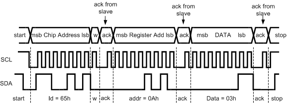
Every byte put on the SDA line must be eight bits long, with the most significant bit (MSB) transferred first. Each byte of data has to be followed by an acknowledge bit. The acknowledge related clock pulse is generated by the master. The master releases the SDA line (HIGH) during the acknowledge clock pulse. The LM3645 pulls down the SDA line during the 9th clock pulse, signifying an acknowledge. The LM3645 generates an acknowledge after each byte is received. There is no acknowledge created after data is read from the device.
After the START condition, the I2C master sends a chip address. This address is seven bits long followed by an eighth bit which is a data direction bit (R/W). The LM3645 7-bit address is 0x65. For the eighth bit, a '0' indicates a WRITE and a '1' indicates a READ. The second byte selects the register to which the data is written. The third byte contains data to write to the selected register.
 Figure 6-13 Write Cycle W = Write (SDA = "0") R = Read (SDA = "1") Ack = Acknowledge (SDA Pulled Down by Either Master or Slave) ID = Chip Address, 65h for LM3645