SNVSCV4 September 2024 LM3645
PRODUCTION DATA
- 1
- 1 Features
- 2 Applications
- 3 Description
- 4 Pin Configuration and Functions
- 5 Specifications
-
6 Detailed Description
- 6.1 Overview
- 6.2 Functional Block Diagram
- 6.3
Feature Description
- 6.3.1 Power Amplifier Synchronization (TORCH/TX)
- 6.3.2 Input Voltage Flash Monitor (IVFM)
- 6.3.3
Fault/Protections
- 6.3.3.1 Fault Operation
- 6.3.3.2 Flash Time-Out
- 6.3.3.3 Overvoltage Protection (OVP)
- 6.3.3.4 Current Limit
- 6.3.3.5 NTC Thermistor Input/Outputs (TEMP1, TEMP2)
- 6.3.3.6 Thermal Scale Back
- 6.3.3.7 Thermal Shutdown (TSD)
- 6.3.3.8 Undervoltage Lockout (UVLO)
- 6.3.3.9 LED and/or VOUT Short Fault
- 6.3.3.10 Fault Behavior Table
- 6.4 Device Functioning Modes
- 6.5 Programming and Control
- 6.6 Register Descriptions
- 7 Application and Implementation
- 8 Power Supply Recommendations
- 9 Layout
- 10Device and Documentation Support
- 11Revision History
- 12Mechanical, Packaging, and Orderable Information
6.3.3.4 Current Limit
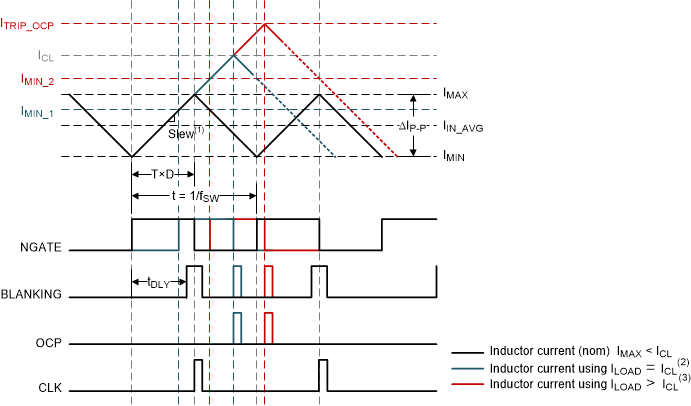
The LM3645 features four selectable inductor current limits that are programmable through the I2C-compatible interface. When the inductor current limit is reached, the LM3645 terminates the charging phase of the switching cycle. Switching resumes at the start of the next switching period. If the overcurrent condition persists, the device operates continuously in current limit.
Since the current limit is sensed in the NMOS switch, there is no mechanism to limit the current when the device operates in Pass Mode (current does not flow through the NMOS in pass mode). In Boost mode or Pass mode if VOUT falls below 2.3 V, the device stops switching, and the P-channel MOSFET operates as a current source limiting the current to 200 mA. This prevents damage to the LM3645 and excessive current draw from the battery during output short-circuit conditions. The output enable bits are not cleared upon a Current Limit event, but a flag is set (bit [4] in reg 0x14).
The over current protection (OCP) circuit compares the inductor current to the input current limit (ICL) setting after a fixed blanking time of tDLY. The blanking time ensures that the OCP signal does not false fire as the low-side NMOS of the boost converter turns on. Use Equation 1 to estimate the maximum recommended total LED current to ensure proper current limit level operation accounting for the delay time.

where
- D is the duty cycle
- η is the boost efficiency
- ICL is the current limit setting
- L is the inductance value
- fSW is the boost switching frequency

