SNVSCV4 September 2024 LM3645
PRODUCTION DATA
- 1
- 1 Features
- 2 Applications
- 3 Description
- 4 Pin Configuration and Functions
- 5 Specifications
-
6 Detailed Description
- 6.1 Overview
- 6.2 Functional Block Diagram
- 6.3
Feature Description
- 6.3.1 Power Amplifier Synchronization (TORCH/TX)
- 6.3.2 Input Voltage Flash Monitor (IVFM)
- 6.3.3
Fault/Protections
- 6.3.3.1 Fault Operation
- 6.3.3.2 Flash Time-Out
- 6.3.3.3 Overvoltage Protection (OVP)
- 6.3.3.4 Current Limit
- 6.3.3.5 NTC Thermistor Input/Outputs (TEMP1, TEMP2)
- 6.3.3.6 Thermal Scale Back
- 6.3.3.7 Thermal Shutdown (TSD)
- 6.3.3.8 Undervoltage Lockout (UVLO)
- 6.3.3.9 LED and/or VOUT Short Fault
- 6.3.3.10 Fault Behavior Table
- 6.4 Device Functioning Modes
- 6.5 Programming and Control
- 6.6 Register Descriptions
- 7 Application and Implementation
- 8 Power Supply Recommendations
- 9 Layout
- 10Device and Documentation Support
- 11Revision History
- 12Mechanical, Packaging, and Orderable Information
5.7 Switching Characteristics
over operating free-air temperature range (unless otherwise noted)
| PARAMETER | TEST CONDITIONS | MIN | TYP | MAX | UNIT | |
|---|---|---|---|---|---|---|
| ƒSW-MAX | Maximum switching frequency | 2.3 V ≤ VIN ≤ 5.5 V | –6% | 4 | 6% | MHz |
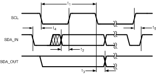
 Figure 5-1 I2C-Compatible Interface Specifications