SNVS250F November 2004 – February 2016 LM3670
PRODUCTION DATA.
- 1 Features
- 2 Applications
- 3 Description
- 4 Revision History
- 5 Connection Diagram
- 6 Specifications
- 7 Detailed Description
- 8 Application and Implementation
- 9 Power Supply Recommendations
- 10Layout
- 11Device and Documentation Support
- 12Mechanical, Packaging, and Orderable Information
8 Application and Implementation
NOTE
Information in the following applications sections is not part of the TI component specification, and TI does not warrant its accuracy or completeness. TI’s customers are responsible for determining suitability of components for their purposes. Customers should validate and test their design implementation to confirm system functionality.
8.1 Application Information
The external control of this device is very easy. First make sure the correct voltage been applied at VIN pin, then simply apply the voltage at EN pin according to the Electrical Characteristics to enable or disable the output voltage.
8.2 Typical Application
8.2.1 Typical Application: Fixed Output
 Figure 17. LM3670 Typical Application, Fixed Output
8.2.1.1 Design Requirements
For typical CMOS voltage regulator applications, use the parameters listed in Table 2.
Table 2. Design Parameters
| DESIGN PARAMETER | EXAMPLE VALUE |
|---|---|
| Minimum input voltage | 2.5 V |
| Minimum output voltage | 1.2 V |
| Maximum load current | 350 mA |
8.2.1.2 Detailed Design Procedure
8.2.1.2.1 Inductor Selection
There are two main considerations when choosing an inductor: the inductor current must not saturate, and the inductor current ripple is small enough to achieve the desired output voltage ripple.
There are two methods to choose the inductor current rating.
8.2.1.2.1.1 Method 1
The total current is the sum of the load and the inductor ripple current. This can be written as


where
- ILOAD = load current
- VIN = input voltage
- L = inductor
- ƒ = switching frequency
- IRIPPLE = peak-to-peak current
8.2.1.2.1.2 Method 2
A more conservative approach is to choose an inductor that can handle the current limit of 700 mA.
Given a peak-to-peak current ripple (IPP) the inductor needs to be at least

A 10-µH inductor with a saturation current rating of at least 800 mA is recommended for most applications. Resistance of the inductor resistance must be less than around 0.3 Ω for good efficiency. Table 3 lists suggested inductors and suppliers. For low-cost applications, an unshielded bobbin inductor is suggested. For noise critical applications, a toroidal or shielded-bobbin inductor must be used. A good practice is to lay out the board with overlapping footprints of both types for design flexibility. This allows substitution of a low-noise toroidal inductor, in the event that noise from low-cost bobbin models is unacceptable.
8.2.1.2.2 Input Capacitor Selection
A ceramic input capacitor of 4.7 µF is sufficient for most applications. A larger value may be used for improved input voltage filtering. The input filter capacitor supplies current to the PFET switch of the LM3670 in the first half of each cycle and reduces voltage ripple imposed on the input power source. The low equivalent series resistance (ESR) of a ceramic capacitor provides the best noise filtering of the input voltage spikes due to this rapidly changing current. Select an input filter capacitor with a surge current rating sufficient for the power-up surge from the input power source. The power-up surge current is approximately the value of the capacitor (µF) times the voltage rise rate (V/µs). The input current ripple can be calculated by :

8.2.1.2.3 Output Capacitor Selection
The output filter capacitor smooths out current flow from the inductor to the load, maintaining a steady output voltage during transient load changes and reduces output voltage ripple. These capacitors must be selected with sufficient capacitance and sufficiently low ESR to perform these functions.
The output ripple current can be calculated as:
Voltage peak-to-peak ripple due to capacitance = 
Voltage peak-to-peak ripple due to ESR = 
Voltage peak-to-peak ripple, root mean squared = 
Note that the output ripple is dependent on the current ripple and the equivalent series resistance of the output capacitor (RESR).
Because these two components are out-of-phase the RMS value is used. The RESR is frequency dependent (as well as temperature dependent); make sure the frequency of the RESR given is the same order of magnitude as the switching frequency.
8.2.1.3 Application Curves
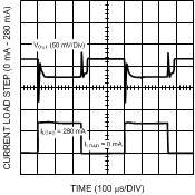
| ILOAD = 0 mA to 280 mA | ||
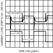
| ILOAD = 0 mA to 350 mA | ||
8.2.2 Typical Application: Adjustable Output
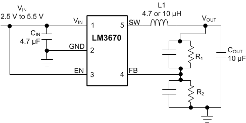 Figure 20. LM3670 Typical Application: Adjustable Output
8.2.2.1 Design Requirements
For adjustable LM3670 option, use the design parameters in Table 5
Table 5. Design Parameters
| DESIGN PARAMETER | EXAMPLE VALUE |
|---|---|
| Input voltage range | 2.5 V to 5.5 |
| Input capacitor | 4.7 µF |
| Output capacitor | 10 µF |
| Inductor | 4.7 µH or 10 µH |
| ADJ programmable output voltage | 0.7 V to 2.5 V |
8.2.2.2 Detailed Design Procedure
8.2.2.2.1 Output Voltage Selection for Adjustable LM3670
The output voltage of the adjustable parts can be programmed through the resistor network connected from VOUT to VFB then to GND. VOUT is adjusted to make VFB equal to 0.5 V. The resistor from VFB to GND (R2) must be at least 100 KΩ to keep the current sunk through this network well below the 15-µA quiescent current level (PFM mode with no switching) but large enough that it is not susceptible to noise. If R2 is 200 KΩ, and VFB is 0.5 V, then the current through the resistor feedback network is 2.5 µA (IFB = 0.5 V / R2). The output voltage formula is:

where
- VOUT = output voltage (V)
- VFB = feedback voltage (0.5 V typical)
- R1 Resistor from VOUT to VFB (Ω)
- R2 Resistor from VOUT to GND (Ω)
For output voltage greater than or equal to 0.7 V a frequency zero must be added at 10 kHz for stability.

For any output voltages equal to 0.7 V or 2.5 V, a pole must also be placed at 10 kHz (see Table 6).
Table 6. Adjustable LM3670 Configurations for Various VOUT
| VOUT (V) | R1 (KΩ) | R2 (KΩ) | C1 (pF) | C2 (pF) | L (µH) | CIN (µF) | COUT (µF) |
|---|---|---|---|---|---|---|---|
| 0.7 | 80.6 | 200 | 200 | 150 | 4.7 | 4.7 | 10 |
| 0.8 | 120 | 200 | 130 | none | 4.7 | 4.7 | 10 |
| 0.9 | 160 | 200 | 100 | none | 4.7 | 4.7 | 10 |
| 1.0 | 200 | 200 | 82 | none | 4.7 | 4.7 | 10 |
| 1.1 | 240 | 200 | 68 | none | 4.7 | 4.7 | 10 |
| 1.2 | 280 | 200 | 56 | none | 4.7 | 4.7 | 10 |
| 1.24 | 221 | 150 | 75 | 120 | 4.7 | 4.7 | 10 |
| 1.5 | 402 | 200 | 39 | none | 10 | 4.7 | 10 |
| 1.6 | 442 | 200 | 39 | none | 10 | 4.7 | 10 |
| 1.7 | 487 | 200 | 33 | none | 10 | 4.7 | 10 |
| 1.875 | 549 | 200 | 30 | none | 10 | 4.7 | 14.7(1) |
| 2.5 | 806 | 200 | 22 | 82 | 10 | 4.7 | 22 |
8.2.2.3 Application Curves
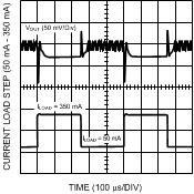
| ILOAD = 50 mA to 350 mA | ||
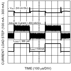
| ILOAD = 100 mA to 300 mA | ||