JAJSH28D November 2013 – March 2019 LM3697
PRODUCTION DATA.
- 1 特長
- 2 アプリケーション
- 3 概要
- 4 改訂履歴
- 5 Pin Configuration and Functions
- 6 Specifications
-
7 Detailed Description
- 7.1 Overview
- 7.2 Functional Block Diagram
- 7.3 Feature Descriptions
- 7.4 Device Functional Modes
- 7.5 Register Maps
- 8 Application and Implementation
- 9 Power Supply Recommendations
- 10Layout
- 11デバイスおよびドキュメントのサポート
- 12メカニカル、パッケージ、および注文情報
パッケージ・オプション
デバイスごとのパッケージ図は、PDF版データシートをご参照ください。
メカニカル・データ(パッケージ|ピン)
- YFQ|12
サーマルパッド・メカニカル・データ
発注情報
10.1 Layout Guidelines
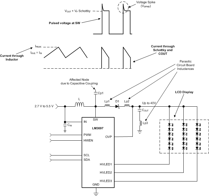
The LM3697 device's inductive boost converter sees a high switched voltage (up to VOVP) at the SW pin, and a step current (up to ICL_BOOST) through the Schottky diode and output capacitor each switching cycle. The high switching voltage can create interference into nearby nodes due to electric field coupling (I = CdV/dt). The large step current through the diode and the output capacitor can cause a large voltage spike at the SW pin and the OVP pin due to parasitic inductance in the step current conducting path (V = Ldi/dt). Board layout guidelines are geared towards minimizing this electric field coupling and conducted noise. Figure 57 highlights these two noise-generating components.
 Figure 57. LM3697 Inductive Boost Converter Showing Pulsed Voltage at SW (High Dv/Dt) and Current Through Schottky And COUT (High Di/Dt)
 The following list details the main (layout sensitive) areas of the LM3697 device’s inductive boost converter in order of decreasing importance:
- Output Capacitor
- Schottky Cathode to COUT+
- COUT− to GND
- Schottky Diode
- SW pin to Schottky Anode
- Schottky Cathode to COUT+
- Inductor
- SW Node PCB capacitance to other traces
- Input Capacitor
- CIN+ to IN terminal