JAJSH28D November 2013 – March 2019 LM3697
PRODUCTION DATA.
- 1 特長
- 2 アプリケーション
- 3 概要
- 4 改訂履歴
- 5 Pin Configuration and Functions
- 6 Specifications
-
7 Detailed Description
- 7.1 Overview
- 7.2 Functional Block Diagram
- 7.3 Feature Descriptions
- 7.4 Device Functional Modes
- 7.5 Register Maps
- 8 Application and Implementation
- 9 Power Supply Recommendations
- 10Layout
- 11デバイスおよびドキュメントのサポート
- 12メカニカル、パッケージ、および注文情報
パッケージ・オプション
デバイスごとのパッケージ図は、PDF版データシートをご参照ください。
メカニカル・データ(パッケージ|ピン)
- YFQ|12
サーマルパッド・メカニカル・データ
発注情報
10.1.4 Boost Input Capacitor Placement
For the LM3697 device’s boost converter, the input capacitor filters the inductor current ripple and the internal MOSFET driver currents during turnon of the internal power switch. The driver current requirement can range from 50 mA at 2.7 V to over 200 mA at 5.5 V with fast durations of approximately 10 ns to 20 ns. This appears as high di/dt current pulses coming from the input capacitor each time the switch turns on. Close placement of the input capacitor to the IN pin and to the GND in is critical because any series inductance between IN and CIN+ or CIN− and GND can create voltage spikes that could appear on the VIN supply line and in the GND plane.
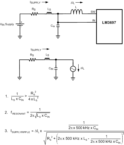
Close placement of the input bypass capacitor at the input side of the inductor is also critical. The source impedance (inductance and resistance) from the input supply, along with the input capacitor of the LM3697, forms a series RLC circuit. If the output resistance from the source (RS) is low enough the circuit is underdamped and has a resonant frequency (typically the case). Depending on the size of LS the resonant frequency could occur below, close to, or above the switching frequency of the device. This can cause the supply current ripple to be:
- Approximately equal to the inductor current ripple when the resonant frequency occurs well above the LM3697 device's switching frequency;
- Greater than the inductor current ripple when the resonant frequency occurs near the switching frequency; or
- Less than the inductor current ripple when the resonant frequency occurs well below the switching frequency.
Figure 58 shows the series RLC circuit formed from the output impedance of the supply and the input capacitor. The circuit is redrawn for the AC case where the VIN supply is replaced with a short to GND, and the LM3697 + Inductor is replaced with a current source (ΔIL). Equation 1 is the criteria for an underdamped response. Equation 2 is the resonant frequency. Equation 3 is the approximated supply current ripple as a function of LS, RS, and CIN.
As an example, consider a 3.6-V supply with 0.1 Ω of series resistance connected to CIN through 50 nH of connecting traces. This results in an underdamped input-filter circuit with a resonant frequency of 712 kHz. Because both the 1-MHz and 500-kHz switching frequency options lie close to the resonant frequency of the input filter, the supply current ripple is probably larger than the inductor current ripple. In this case, using equation 3, the supply current ripple can be approximated as 1.68 times the inductor current ripple (using a 500-kHz switching frequency) and 0.86 times the inductor current ripple using a 1-MHz switching frequency. Increasing the series inductance (LS) to 500 nH causes the resonant frequency to move to around 225 kHz, and the supply current ripple to be approximately 0.25 times the inductor current ripple (500-kHz switching frequency) and 0.053 times for a 1-MHz switching frequency.
 Figure 58. Input RLC Network