SNVS088F May 2004 – April 2016 LM3704
PRODUCTION DATA.
5 Specifications
5.1 Absolute Maximum Ratings
over operating free-air temperature range (unless otherwise noted)(1)| MIN | MAX | UNIT | ||
|---|---|---|---|---|
| Supply voltage, VCC | –0.3 | 6 | V | |
| All other inputs | –0.3 | VCC + 0.3 | V | |
| Power dissipation | See(2) | |||
| Storage temperature, Tstg | –65 | 150 | °C | |
(1) Stresses beyond those listed under Absolute Maximum Ratings may cause permanent damage to the device. These are stress ratings only, which do not imply functional operation of the device at these or any other conditions beyond those indicated under Recommended Operating Conditions. Exposure to absolute-maximum-rated conditions for extended periods may affect device reliability.
(2) The maximum allowable power dissipation is a function of the maximum junction temperature, TJ(MAX), the junction-to-ambient thermal resistance, θJ-A, and the ambient temperature, TA. The maximum allowable power dissipation at any ambient temperature is calculated using:

Where the value of θJ-A for the 10-pin VSSOP package is 195°C/W in a typical printed-circuit board (PCB) mounting and the DSBGA package is 220°C/W.

Where the value of θJ-A for the 10-pin VSSOP package is 195°C/W in a typical printed-circuit board (PCB) mounting and the DSBGA package is 220°C/W.
5.2 ESD Ratings
| VALUE | UNIT | |||
|---|---|---|---|---|
| V(ESD) | Electrostatic discharge | Human-body model (HBM), per ANSI/ESDA/JEDEC JS-001(1) | ±1500 | V |
| Charged-device model (CDM), per JEDEC specification JESD22-C101(2) | ±150 | |||
(1) JEDEC document JEP155 states that 500-V HBM allows safe manufacturing with a standard ESD control process.
(2) JEDEC document JEP157 states that 250-V CDM allows safe manufacturing with a standard ESD control process.
5.3 Recommended Operating Conditions
over operating free-air temperature range (unless otherwise noted)| MIN | MAX | UNIT | ||
|---|---|---|---|---|
| TA | Free-air temperature | –40 | 85 | °C |
5.4 Thermal Information
| THERMAL METRIC(1) | LM3704 | UNIT | |
|---|---|---|---|
| DGS (VSSOP) | |||
| 10 PINS | |||
| RθJA | Junction-to-ambient thermal resistance | 163.7 | °C/W |
| RθJC(top) | Junction-to-case (top) thermal resistance | 58.3 | °C/W |
| RθJB | Junction-to-board thermal resistance | 83.5 | °C/W |
| ψJT | Junction-to-top characterization parameter | 6 | °C/W |
| ψJB | Junction-to-board characterization parameter | 82.2 | °C/W |
| RθJC(bot) | Junction-to-case (bottom) thermal resistance | — | °C/W |
(1) For more information about traditional and new thermal metrics, see the Semiconductor and IC Package Thermal Metrics application report, SPRA953.
5.5 Electrical Characteristics
at TJ = 25°C and VCC = 2.2 V to 5.5 V (unless otherwise noted)| PARAMETER | TEST CONDITIONS | MIN | TYP | MAX | UNIT | ||
|---|---|---|---|---|---|---|---|
| POWER SUPPLY | |||||||
| VCC | Operating voltage | LM3704, TJ = –40°C to 85°C | 1 | 5.5 | V | ||
| ICC | VCC supply current | All inputs = VCC, all outputs floating |
TJ = 25°C | 28 | µA | ||
| TJ = –40°C to 85°C | 50 | ||||||
| RESET THRESHOLD | |||||||
| VRST | Reset threshold | VCC falling | TJ = 25°C | –0.5% | VRST | 0.5% | |
| TJ = –40°C to 85°C | –2% | 2% | |||||
| TJ = 0°C to 70°C | –1.5% | 1.5% | |||||
| VRSTH | Reset threshold hysteresis | 0.0032 × VRST | mV | ||||
| tRP | Reset time-out period | Reset time-out period = C | TJ = 25°C | 200 | ms | ||
| TJ = –40°C to 85°C | 140 | 280 | |||||
| tRD | VCC to reset delay | VCC falling at 1 mV/µs | 20 | µs | |||
| RESET | |||||||
| VOL | RESET | VCC > 1.0 V, ISINK = 50 µA, TJ = –40°C to 85°C |
0.3 | V | |||
| VCC > 1.2 V, ISINK = 100 µA, TJ = –40°C to 85°C |
0.3 | ||||||
| VCC > 2.25 V, ISINK = 900 µA, TJ = –40°C to 85°C |
0.3 | ||||||
| VCC > 2.7 V, ISINK = 1.2 mA, TJ = –40°C to 85°C |
0.3 | ||||||
| VCC > 4.5 V, ISINK = 3.2 mA, TJ = –40°C to 85°C |
0.4 | ||||||
| VOH | RESET | VCC > 2.25 V, ISOURCE = 300 µA, TJ = –40°C to 85°C |
0.8 × VCC | V | |||
| VCC > 2.7 V, ISOURCE = 500 µA, TJ = –40°C to 85°C |
0.8 × VCC | ||||||
| VCC > 4.5 V, ISOURCE = 800 µA, TJ = –40°C to 85°C |
VCC − 1.5 | ||||||
| PFI/MR | |||||||
| VPFT | PFI input threshold | TJ = 25°C | 1.225 | V | |||
| TJ = –40°C to 85°C | 1.2 | 1.25 | |||||
| VMRT | MR Input threshold | TJ = –40°C to 85°C | MR, low | 0.8 | V | ||
| MR, high | 2 | ||||||
| VPFTH/ VMRTH |
PFI/MR threshold hysteresis | PFI/MR falling, VCC = VRST MAX to 5.5 V | 0.0032 × VRST | mV | |||
| IPFI | Input current (PFI only) | TJ = –40°C to 85°C | –75 | 75 | nA | ||
| RMR | MR pullup resistance | TJ = 25°C | 56 | kΩ | |||
| TJ = –40°C to 85°C | 35 | 75 | |||||
| tMD | MR to reset delay | 12 | µS | ||||
| tMR | MR pulse width | TJ = –40°C to 85°C | 25 | µS | |||
| PFO, LLO | |||||||
| VOL | PFO, LLO output low voltage | VCC > 2.25 V, ISINK = 900 µA, TJ = –40°C to 85°C |
0.3 | V | |||
| VCC > 2.7 V, ISINK = 1.2 mA, TJ = –40°C to 85°C |
0.3 | ||||||
| VCC > 4.5 V, ISINK = 3.2 mA, TJ = –40°C to 85°C |
0.4 | ||||||
| VOH | PFO, LLO output high voltage | VCC > 2.25 V, ISOURCE = 300 µA, TJ = –40°C to 85°C |
0.8 VCC | V | |||
| VCC > 2.7 V, ISOURCE = 500 µA, TJ = –40°C to 85°C |
0.8 VCC | ||||||
| VCC > 4.5 V, ISOURCE = 800 µA, TJ = –40°C to 85°C |
VCC − 1.5 | ||||||
| LLO OUTPUT | |||||||
| VLLOT | LLO output threshold | VLLO − VRST, VCC falling | TJ = 25°C | 1.02 × VRST | V | ||
| TJ = –40°C to 85°C | 1.01 × VRST | 1.03 × VRST | |||||
| VLLOTH | Low-line comparator hysteresis | 0.0032 × VRST | mV | ||||
| tCD | Low-line comparator delay | VCC falling at 1 mV/µs | 20 | µs | |||
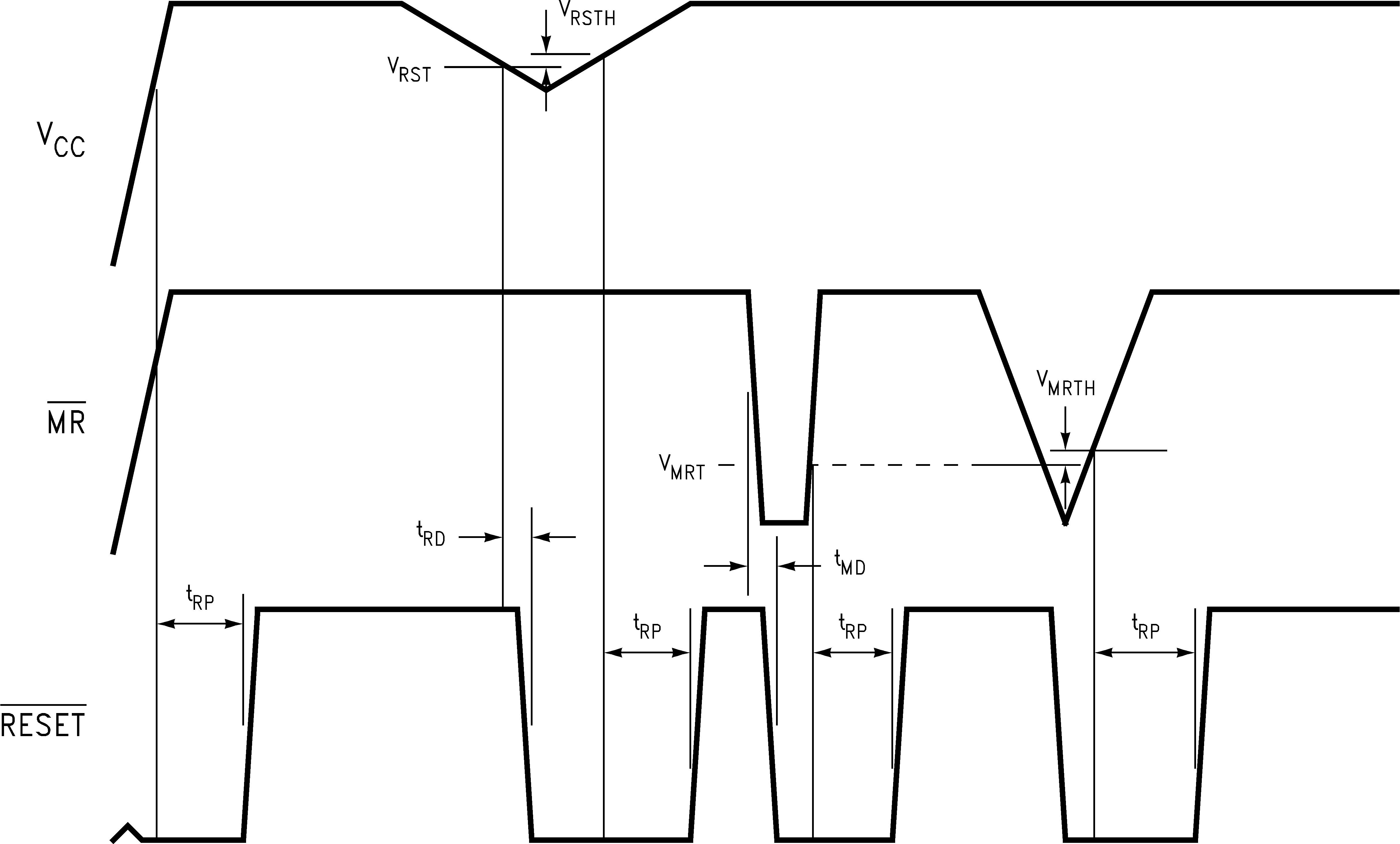 Figure 1. LM3704 Reset Time With MR
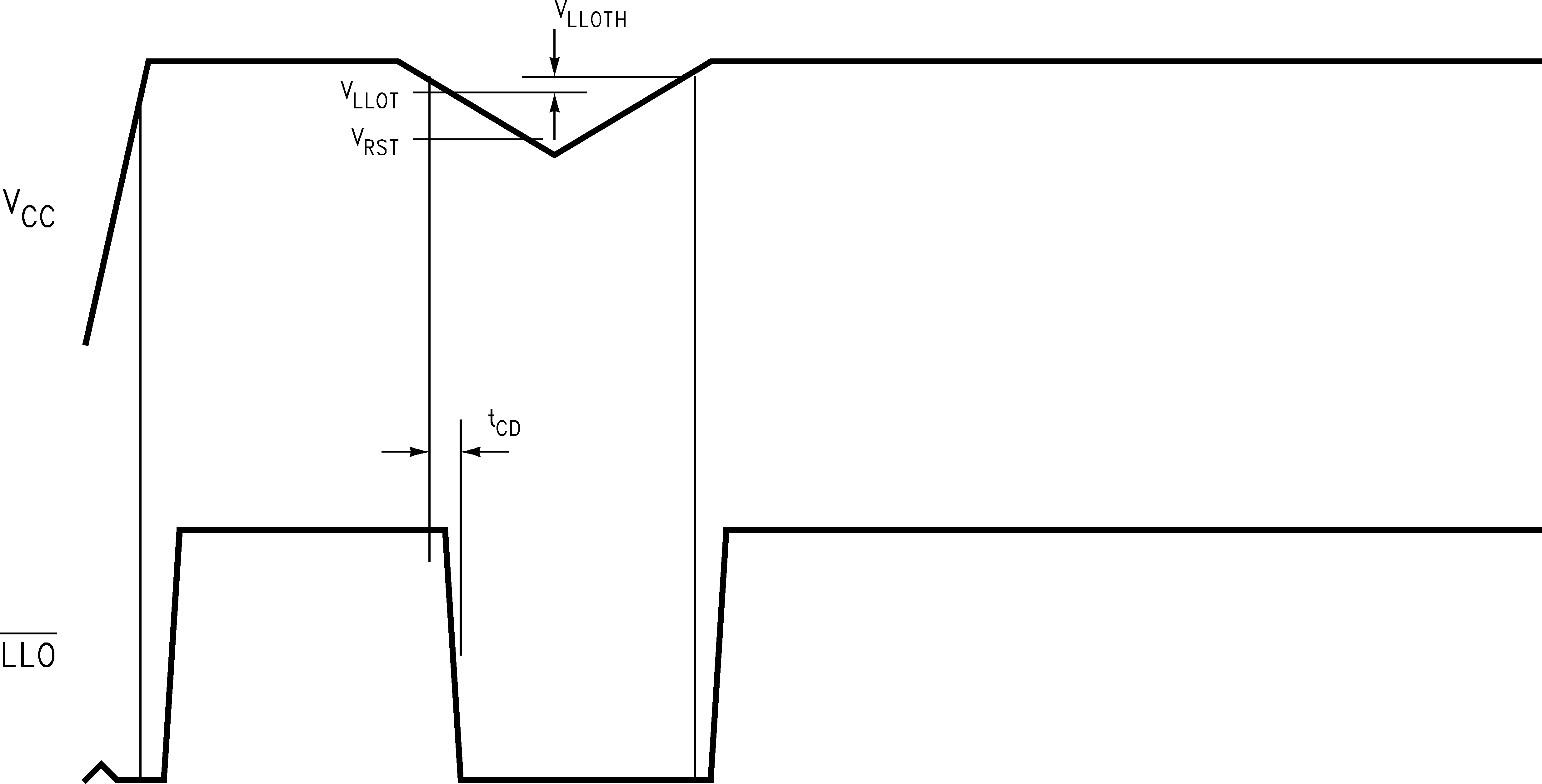 Figure 2. LLO Output
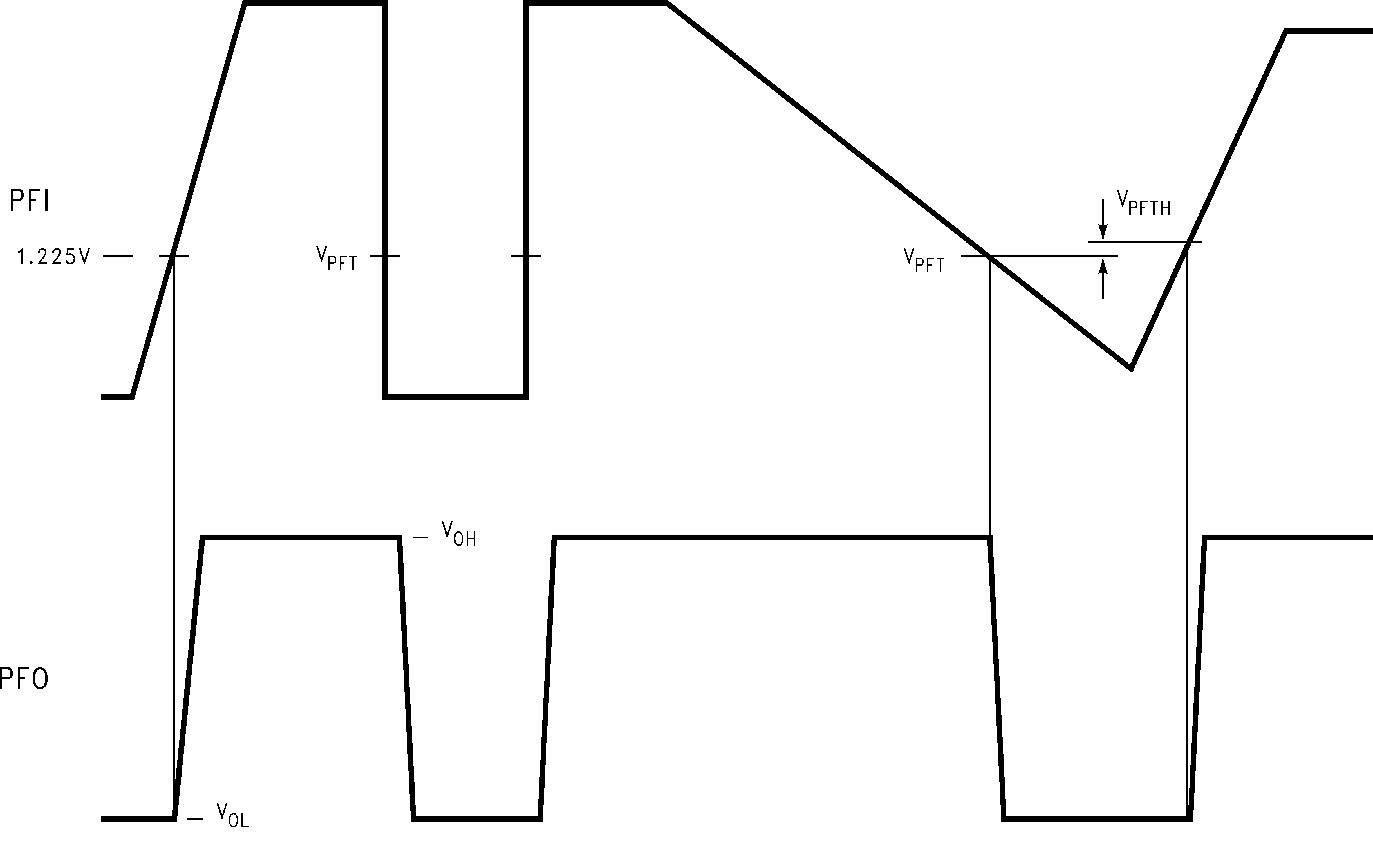 Figure 3. PFI Comparator Timing Diagram
5.6 Typical Characteristics
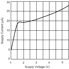 Figure 4. Supply Current vs Supply Voltage
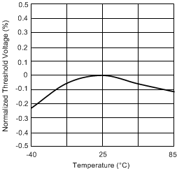 Figure 6. Normalized Reset Threshold Voltage
vs Temperature
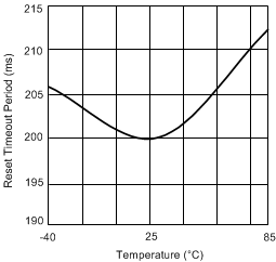
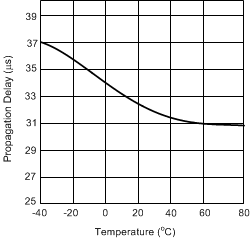 Figure 10. Low-Line Comparator Propagation Delay vs Temperature
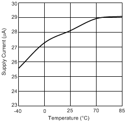 Figure 5. 3.3-V Supply Current vs Temperature
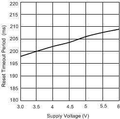 Figure 7. Reset Timeout Period vs VCC
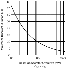
| VCC = 3.3 V |
vs Reset Comparator Overdrive