JAJSAO5I January 2007 – December 2017 LM5022
PRODUCTION DATA.
- 1 特長
- 2 アプリケーション
- 3 概要
- 4 改訂履歴
- 5 Pin Configuration and Functions
- 6 Specifications
- 7 Detailed Description
-
8 Application and Implementation
- 8.1 Application Information
- 8.2
Typical Application
- 8.2.1 Design Requirements
- 8.2.2
Detailed Design Procedure
- 8.2.2.1 Switching Frequency
- 8.2.2.2 MOSFET
- 8.2.2.3 Output Diode
- 8.2.2.4 Boost Inductor
- 8.2.2.5 Output Capacitor
- 8.2.2.6 VCC Decoupling Capacitor
- 8.2.2.7 Input Capacitor
- 8.2.2.8 Current Sense Filter
- 8.2.2.9 RSNS, RS2 and Current Limit
- 8.2.2.10 Control Loop Compensation
- 8.2.2.11 Efficiency Calculations
- 8.2.3 Application Curves
- 9 Power Supply Recommendations
- 10Layout
- 11デバイスおよびドキュメントのサポート
- 12メカニカル、パッケージ、および注文情報
7.4.1 Oscillator, Shutdown, and SYNC
A single external resistor, RT, connected between the RT/SYNC and GND pins sets the LM5022 oscillator frequency. To set the switching frequency (ƒSW), RT can be calculated with Equation 1.
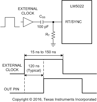
The LM5022 can also be synchronized to an external clock. The external clock must have a higher frequency than the free-running oscillator frequency set by the RT resistor. The clock signal must be capacitively coupled into the RT/SYNC pin with a 100-pF capacitor as shown in Figure 13. A peak voltage level greater than 3.8 V at the RT/SYNC pin is required for detection of the sync pulse. The sync pulse width must be set between 15 ns to 150 ns by the external components. The RT resistor is always required, whether the oscillator is free-running or externally synchronized. The voltage at the RT/SYNC pin is internally regulated to 2 V, and the typical delay from a logic high at the RT/SYNC pin to the rise of the OUT pin voltage is 120 ns. RT must be placed very close to the device and connected directly to the pins of the controller (RT/SYNC and GND).
 Figure 13. SYNC Operation
