JAJSJK6D October 2007 – August 2020 LM5067
PRODUCTION DATA
- 1 特長
- 2 アプリケーション
- 3 概要
- 4 Revision History
- 5 Device Comparison
- 6 Pin Configuration and Functions
- 7 Specifications
- 8 Detailed Description
-
9 Application and Implementation
- 9.1 Application Information
- 9.2
Typical Application
- 9.2.1 Design Requirements
- 9.2.2 Detailed Design Procedure
- 9.2.3 Application Curves
- 10Power Supply Recommendations
- 11Layout
- 12Device and Documentation Support
- 13Mechanical, Packaging, and Orderable Information
パッケージ・オプション
メカニカル・データ(パッケージ|ピン)
サーマルパッド・メカニカル・データ
発注情報
8.1 Overview
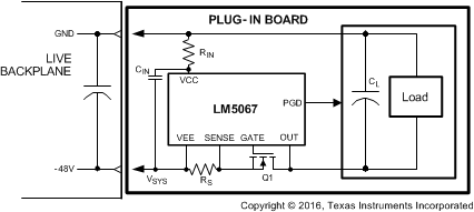
The LM5067 is designed to control the in-rush current to the load upon insertion of a circuit card into a live backplane or other “hot” power source, thereby limiting the voltage sag on the backplane’s supply voltage, and the dV/dt of the voltage applied to the load. Effects on other circuits in the system are minimized, preventing possible unintended resets. During the system power up, the maximum power dissipation in the series pass device is limited to a safe value within the device’s Safe Operating Area (SOA). After the system power up is complete, the LM5067 monitors the load for excessive currents due to a fault or short circuit at the load. Limiting the load current and/or the power in the external MOSFET for an extended period of time results in the shutdown of the series pass MOSFET. After a fault event, the LM5067-1 latches off until the circuit is re-enabled by external control, while the LM5067-2 automatically restarts with defined timing. The circuit breaker function quickly switches off the series pass device upon detection of a severe over-current condition caused by, e.g. a short circuit at the load. The Power Good (PGD) output pin indicates when the output voltage is close to the normal operating value. Programmable undervoltage lock-out (UVLO) and overvoltage lock-out (OVLO) circuits shut down the LM5067 when the system input voltage is outside the desired operating range. The typical configuration of a circuit card with LM5067 hot swap protection is shown in Figure 8-1.
 Figure 8-1 LM5067 Application
The LM5067 can be used in a variety of applications, other than plug-in boards, to monitor for excessive load current, provide transient protection, and ensuring the voltage to the load is within preferred limits. The circuit breaker function protects the system from a sudden short circuit at the load. Use of the UVLO/EN pin allows the LM5067 to be used as a solid state relay. The PGD output provides a status indication of the voltage at the load relative to the input system voltage.