JAJSJK6D October 2007 – August 2020 LM5067
PRODUCTION DATA
- 1 特長
- 2 アプリケーション
- 3 概要
- 4 Revision History
- 5 Device Comparison
- 6 Pin Configuration and Functions
- 7 Specifications
- 8 Detailed Description
-
9 Application and Implementation
- 9.1 Application Information
- 9.2
Typical Application
- 9.2.1 Design Requirements
- 9.2.2 Detailed Design Procedure
- 9.2.3 Application Curves
- 10Power Supply Recommendations
- 11Layout
- 12Device and Documentation Support
- 13Mechanical, Packaging, and Orderable Information
パッケージ・オプション
メカニカル・データ(パッケージ|ピン)
サーマルパッド・メカニカル・データ
発注情報
7.7 Typical Characteristics
Unless otherwise specified the following conditions apply: TJ = 25°C.
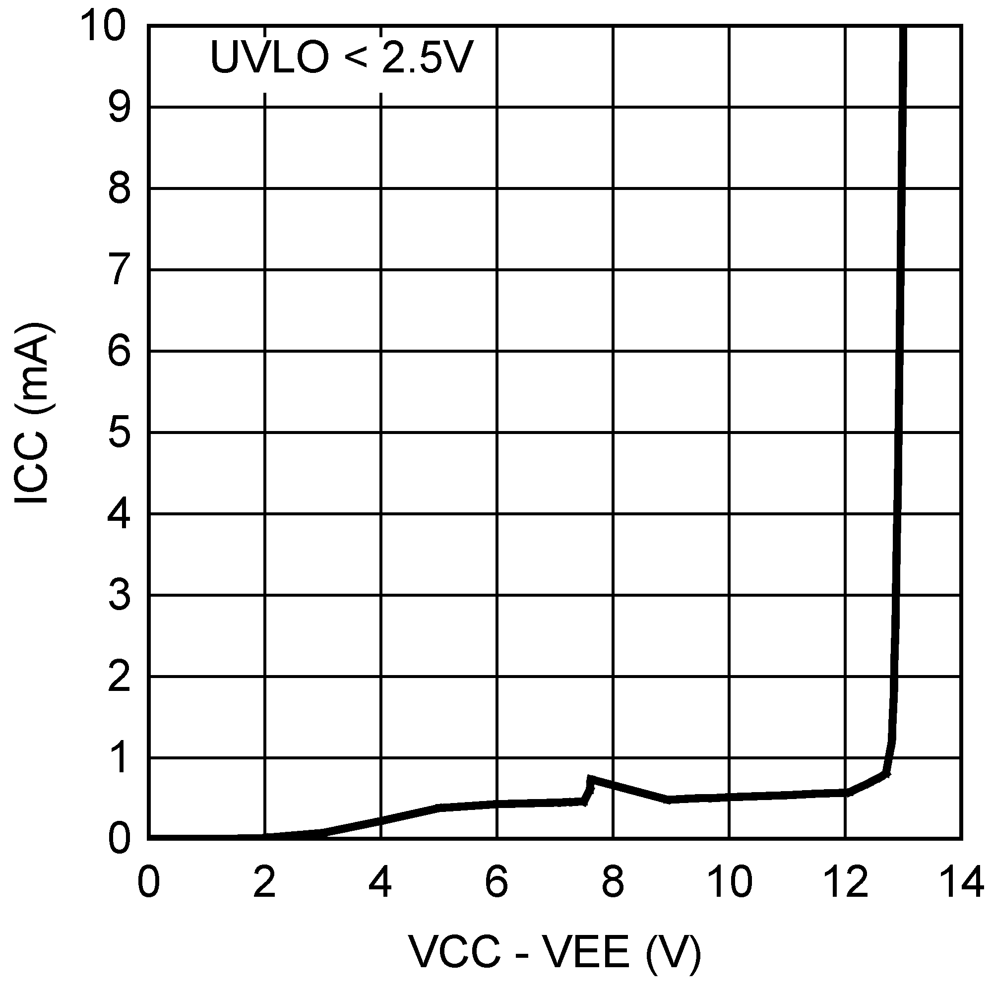 Figure 7-1 ICC vs Operating Voltage - Disabled
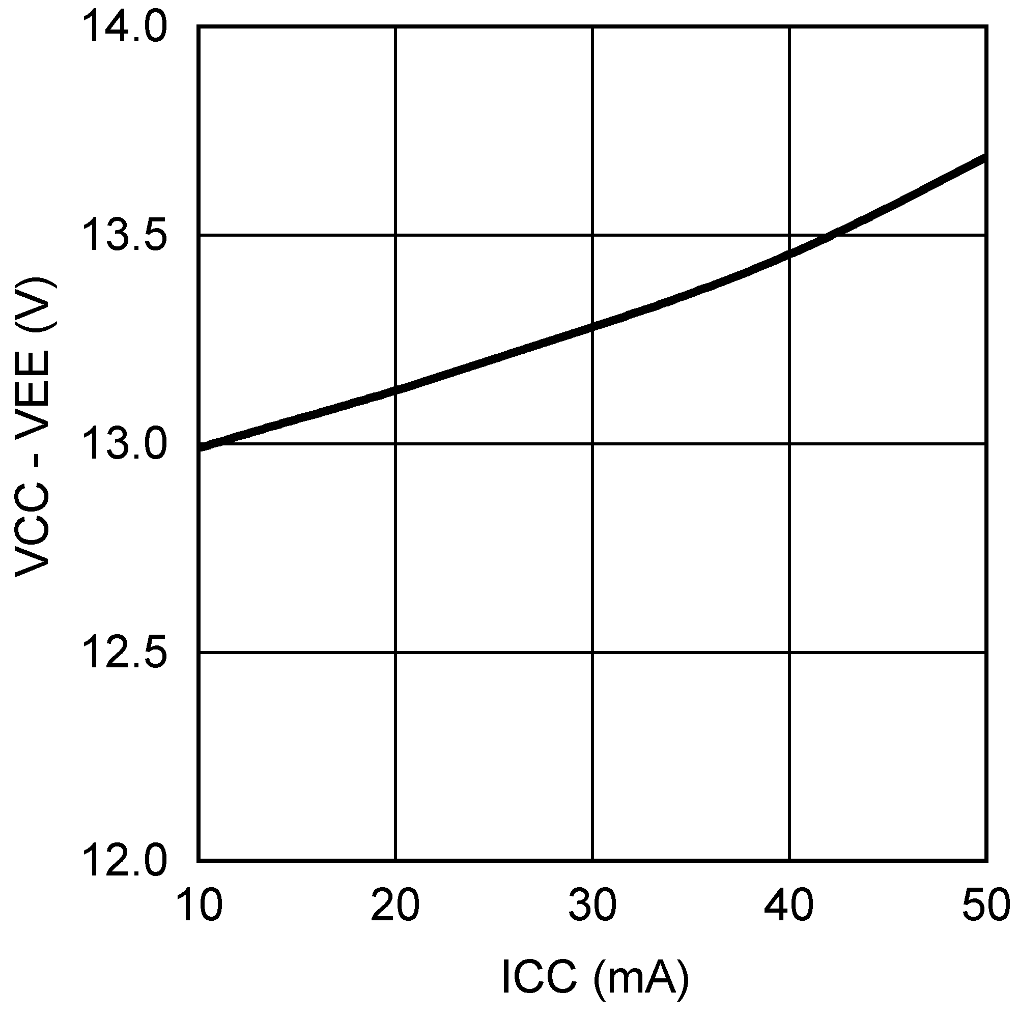 Figure 7-3 Operating Voltage vs ICC
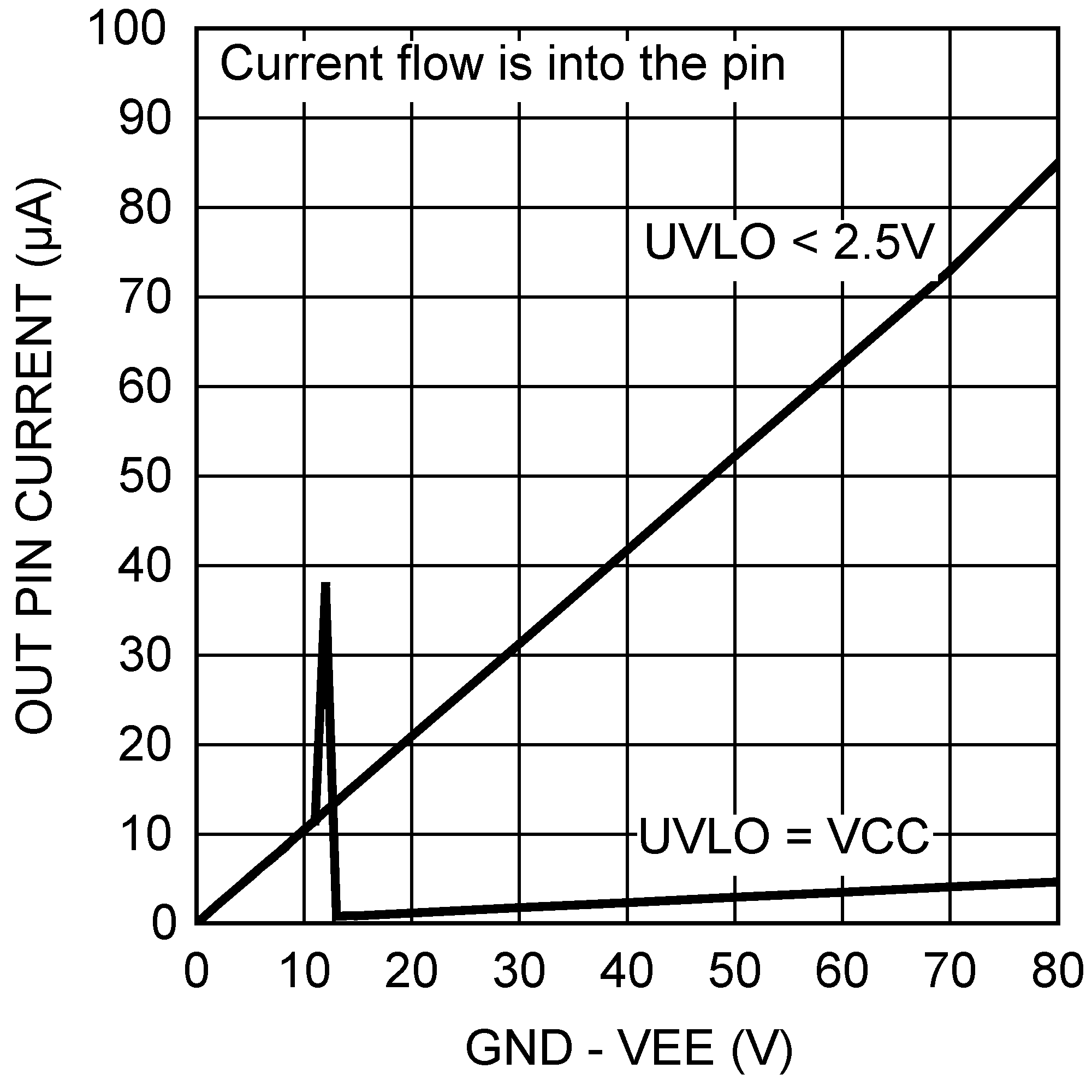 Figure 7-5 OUT Pin Current vs System Voltage
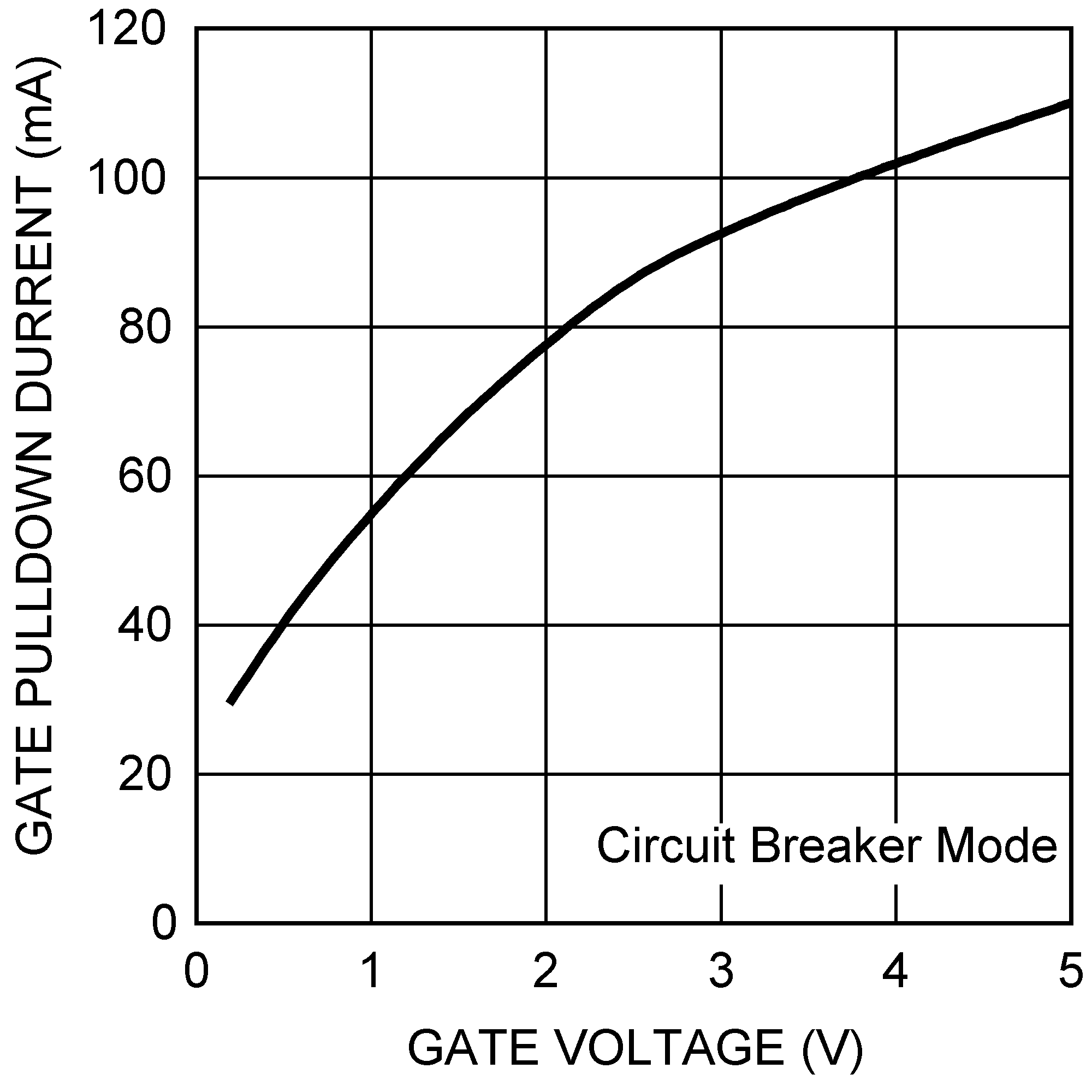 Figure 7-7 GATE Pull-Down Current, Circuit Breaker vs GATE Voltage
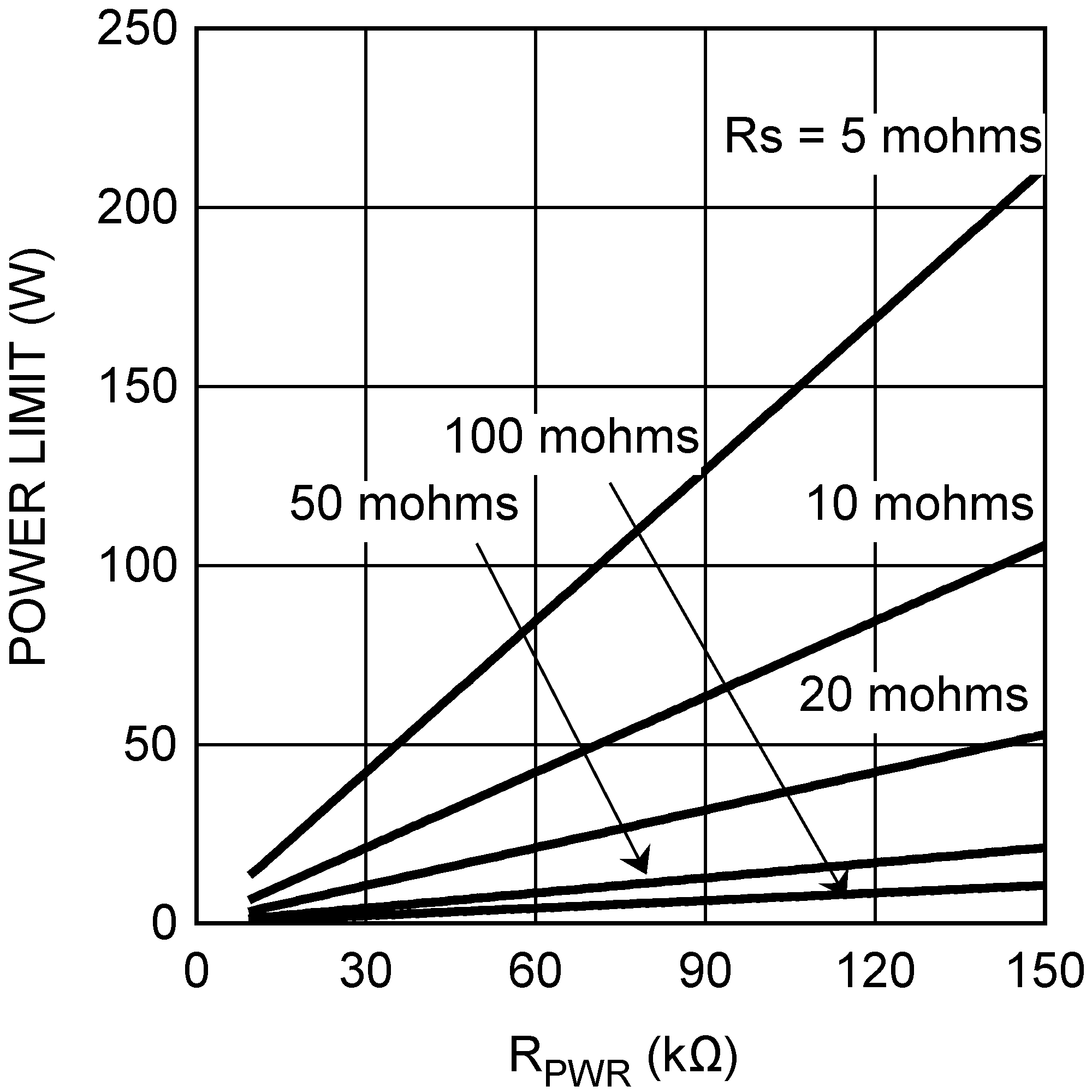 Figure 7-9 MOSFET Power Dissipation Limit vs RPWR and RS
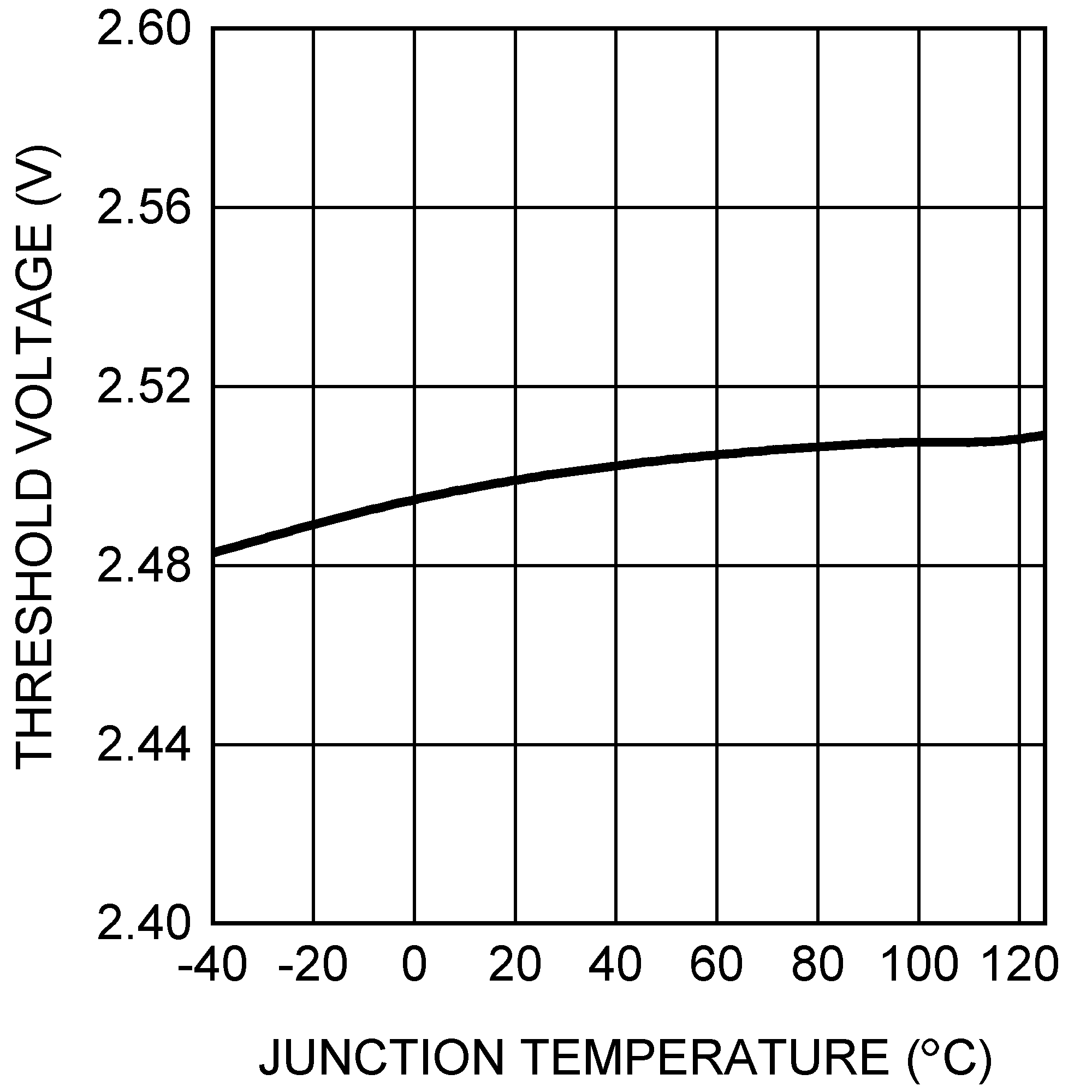 Figure 7-11 UVLO, OVLO Threshold Voltage vs UVLO, OVLO Threshold Voltage
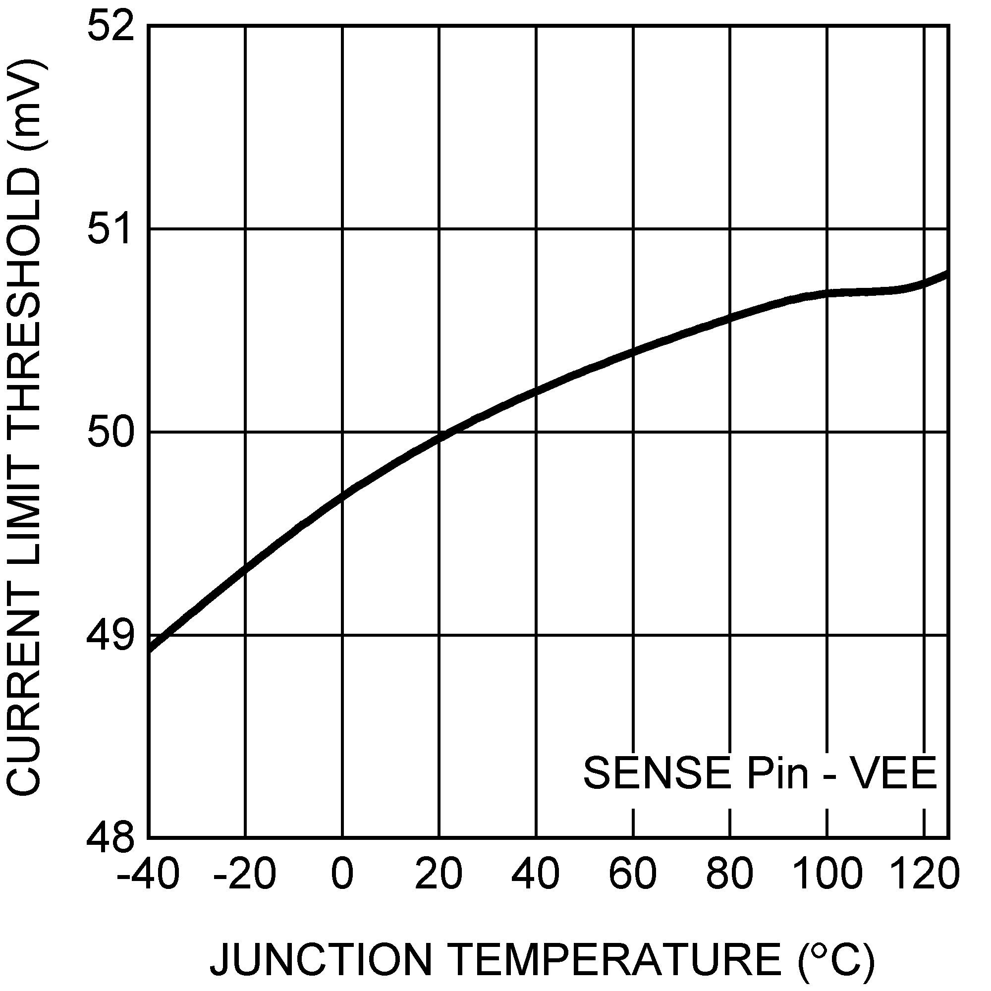 Figure 7-13 Current Limit Threshold vs Temperature
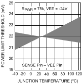 Figure 7-15 Power Limit Threshold vs Temperature
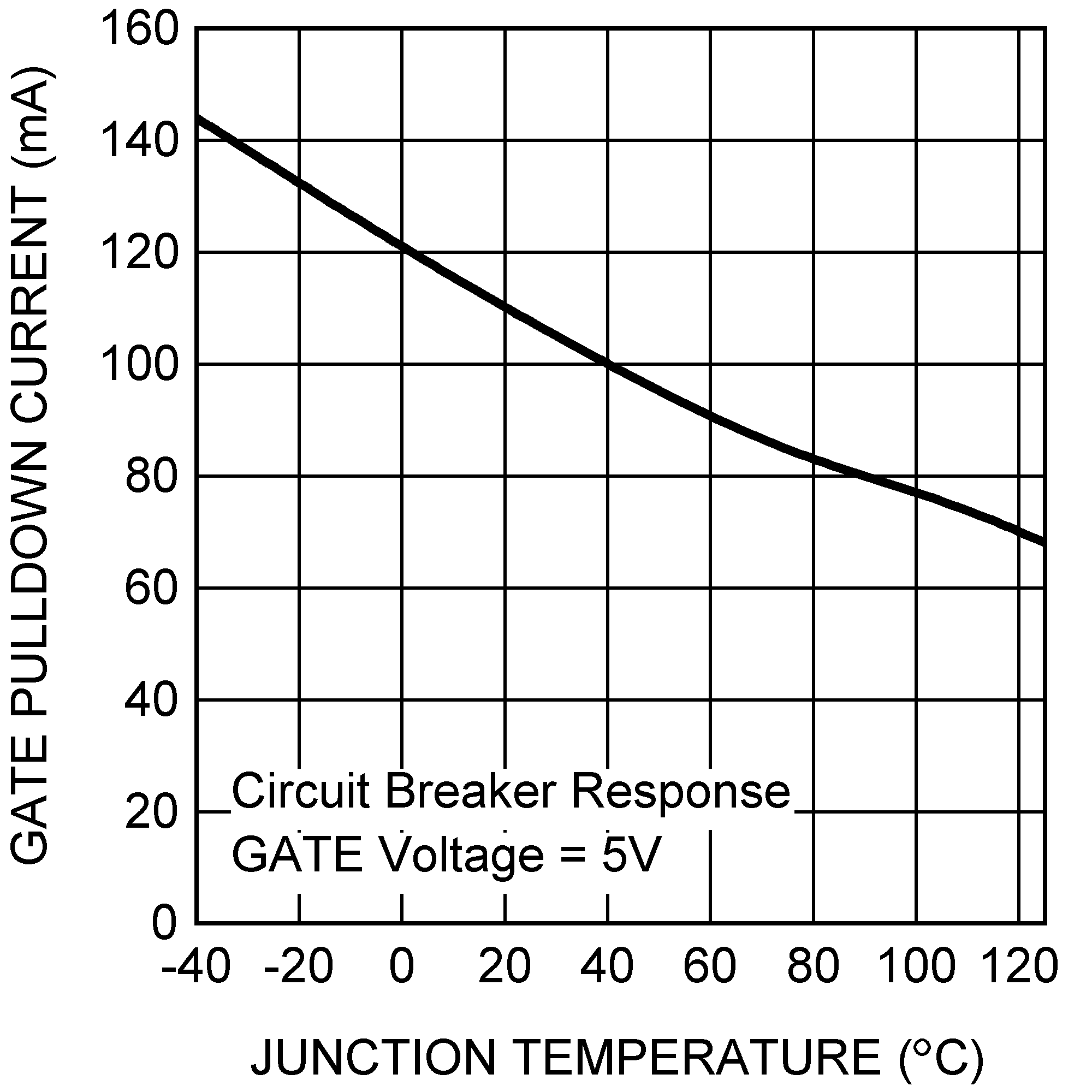 Figure 7-17 GATE Pull-Down Current, Circuit Breaker vs Temperature
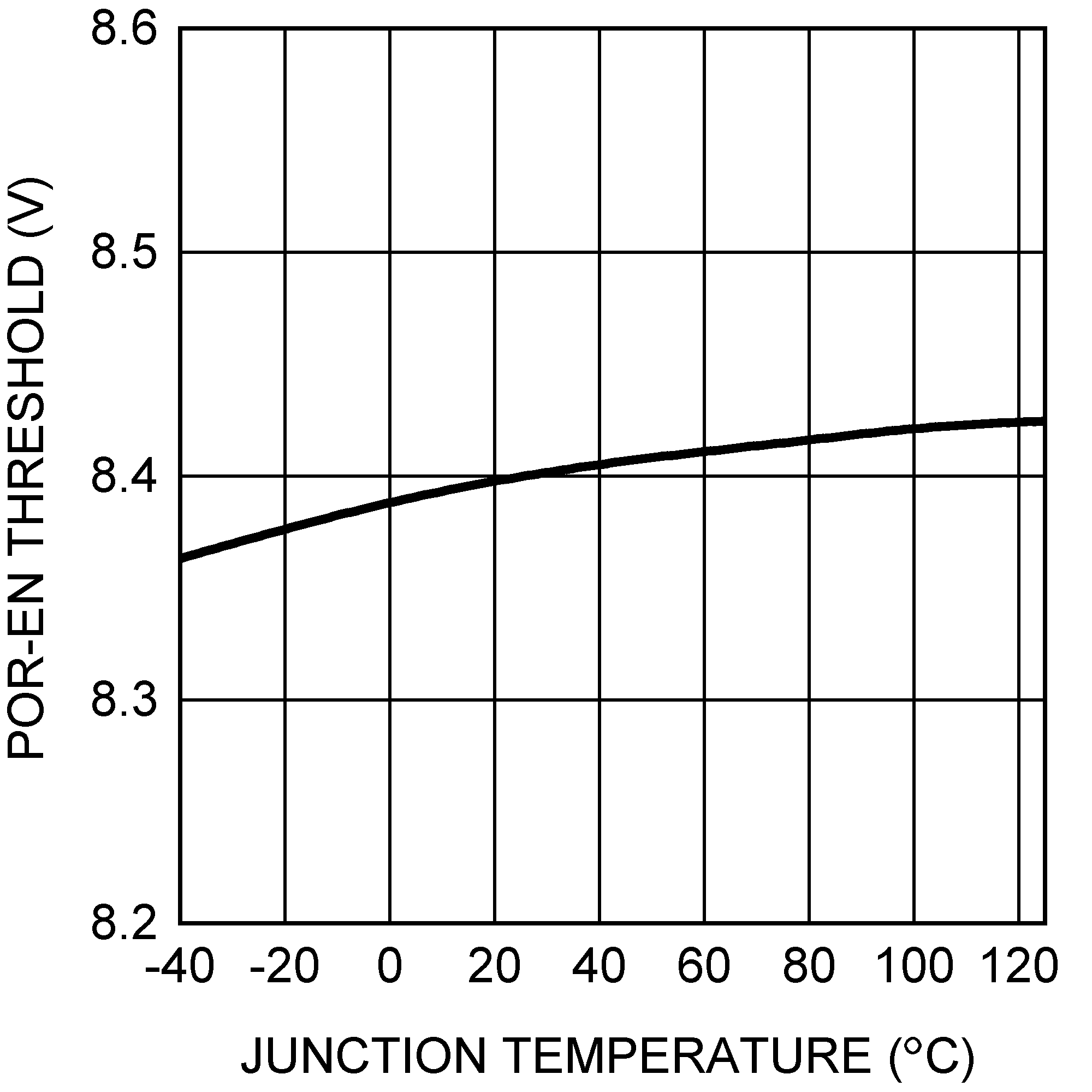 Figure 7-19 POREN Threshold vs Temperature
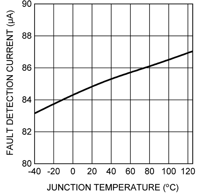 Figure 7-21 TIMER
Pin Fault Detection Current vs Temperature
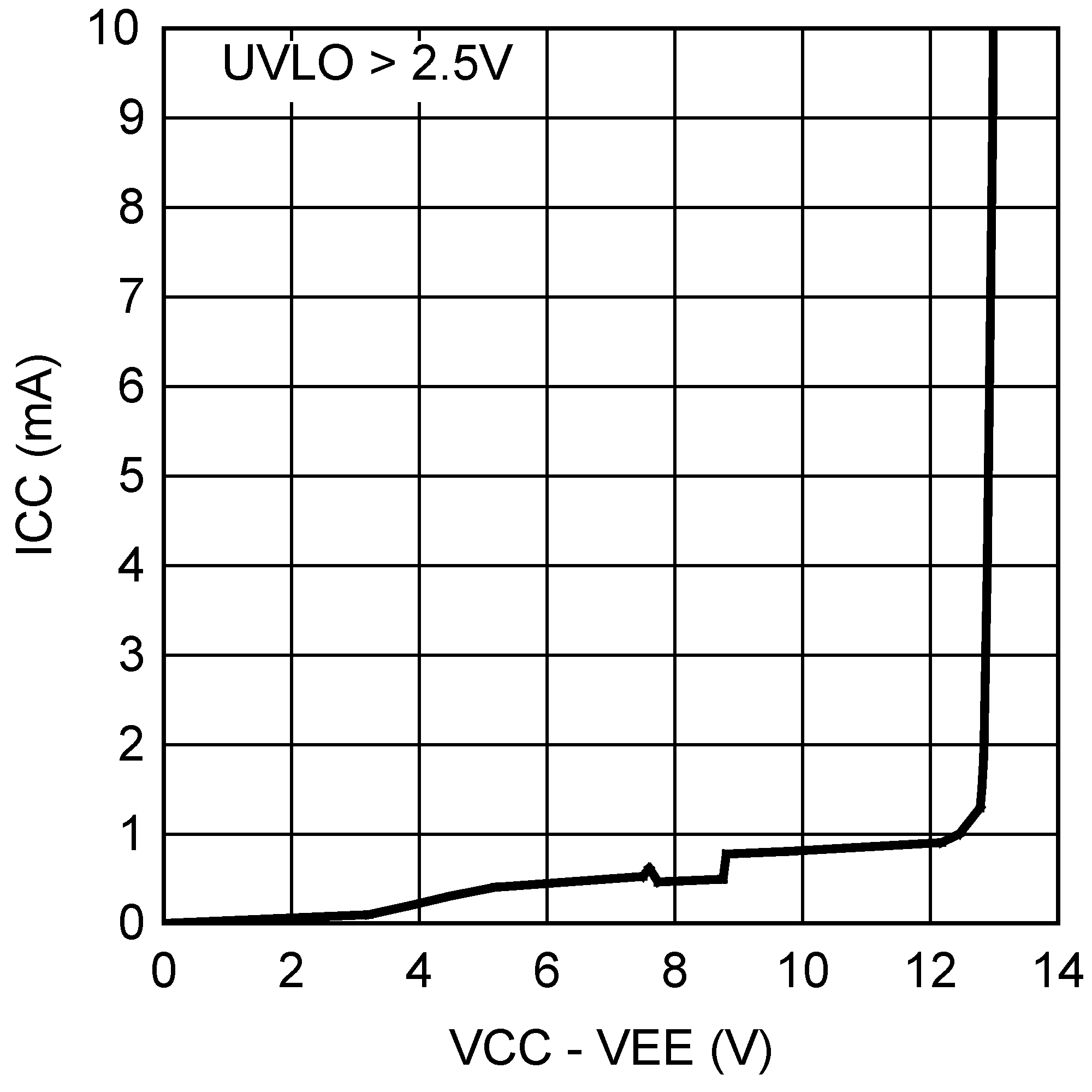 Figure 7-2 ICC vs Operating Voltage - Enabled
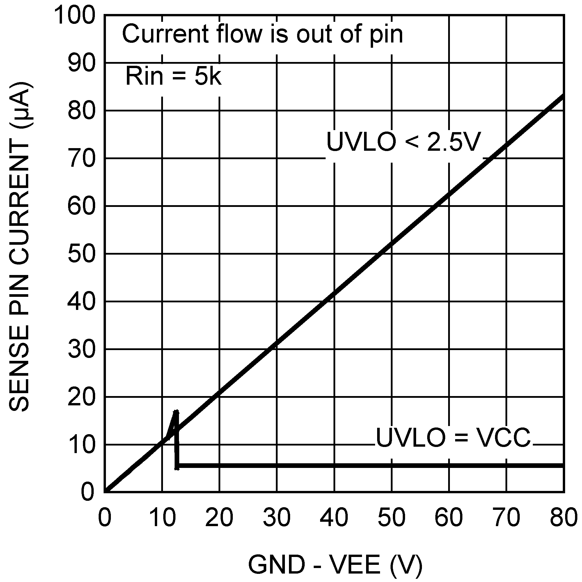 Figure 7-4 SENSE Pin Current vs System Voltage
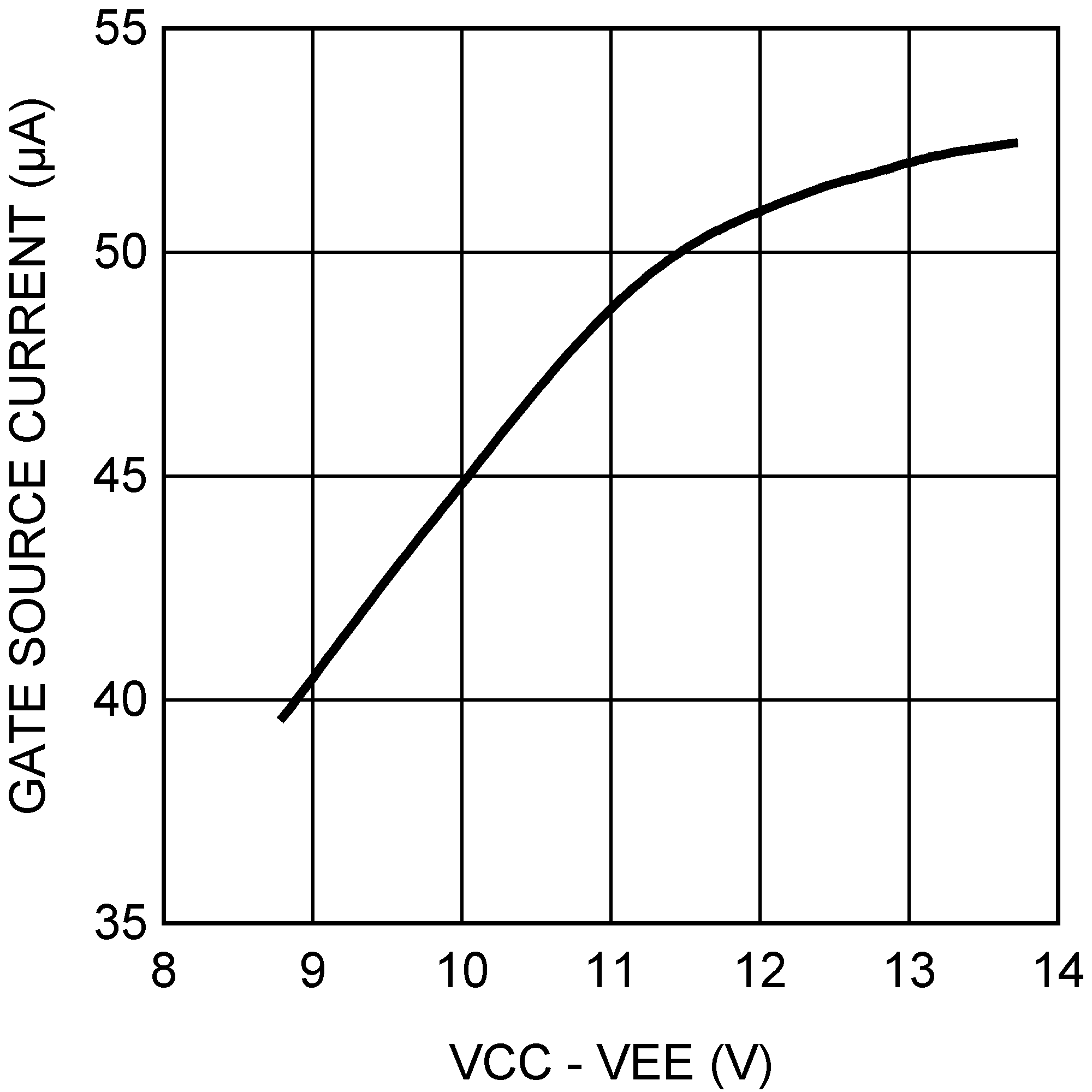 Figure 7-6 GATE Source Current vs Operating Voltage
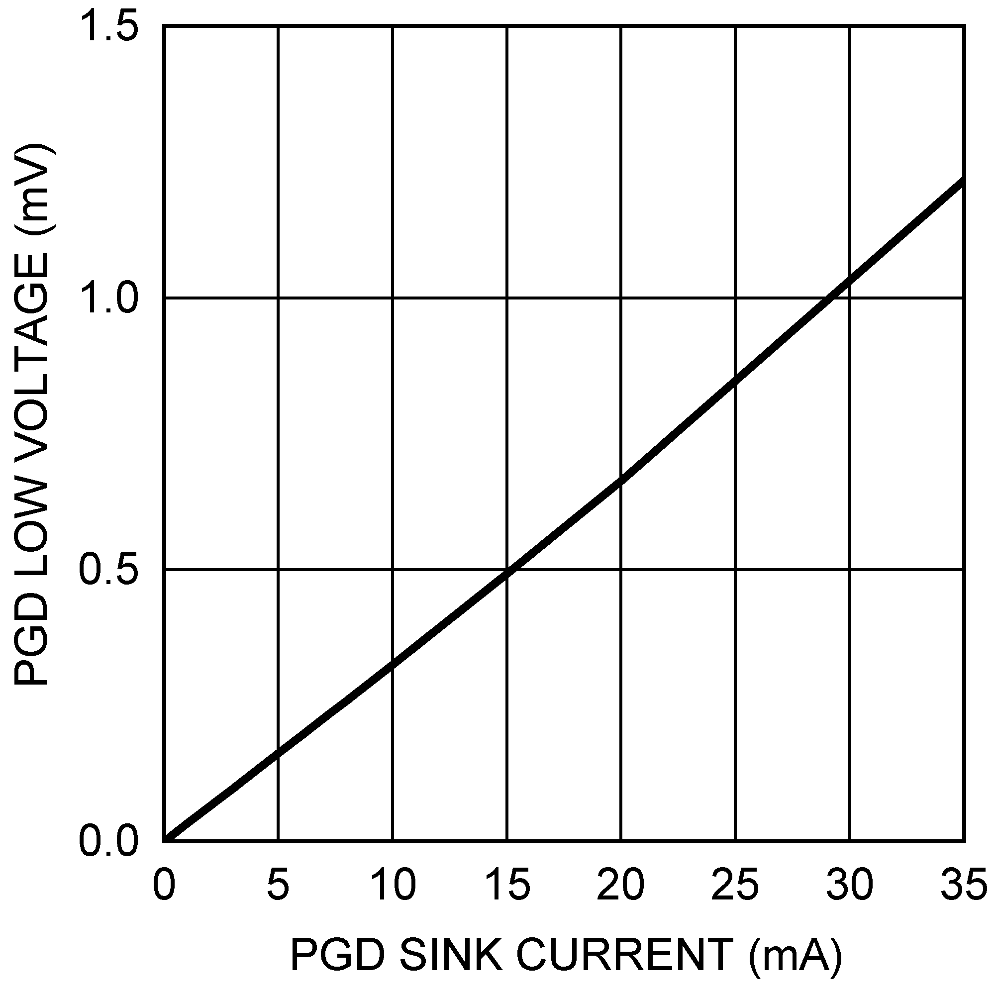 Figure 7-8 PGD Low Voltage vs Sink Current
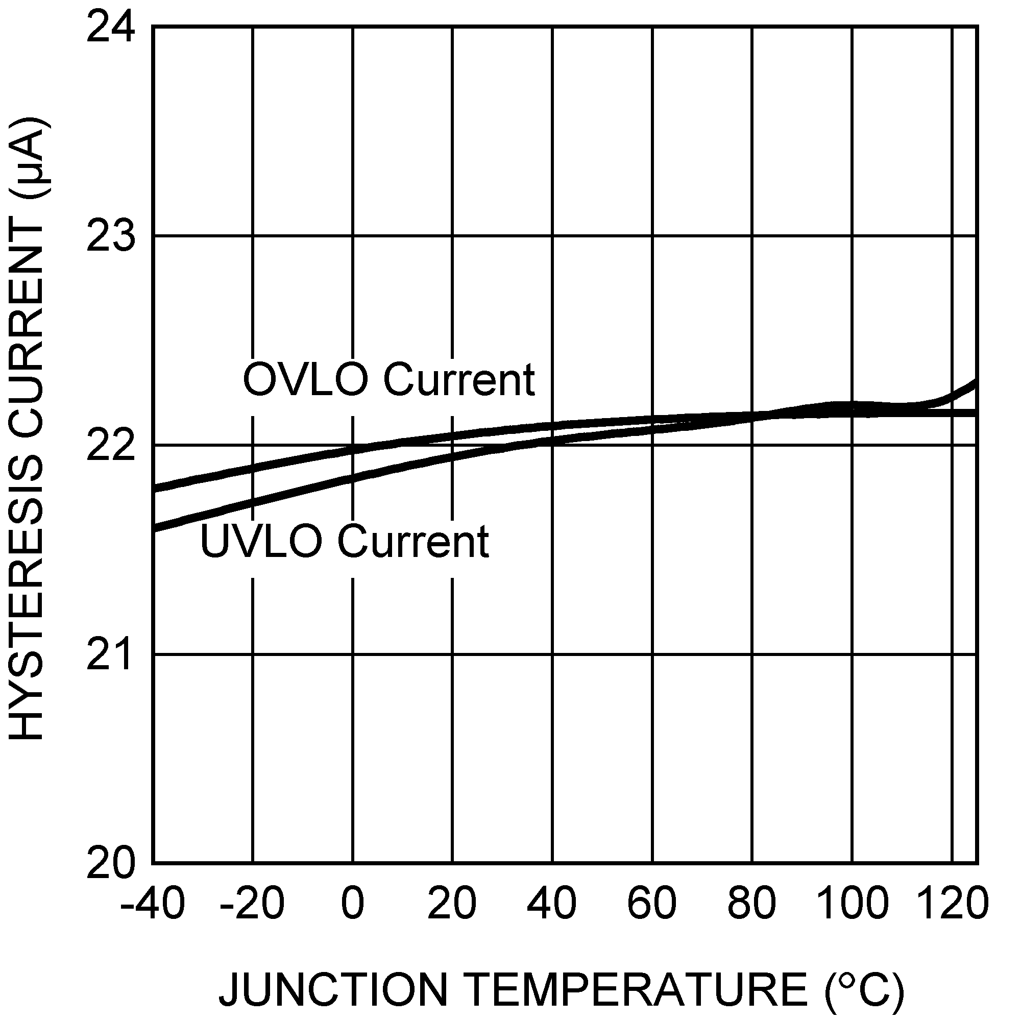 Figure 7-10 UVLO and OVLO Hysteresis Current vs Temperature
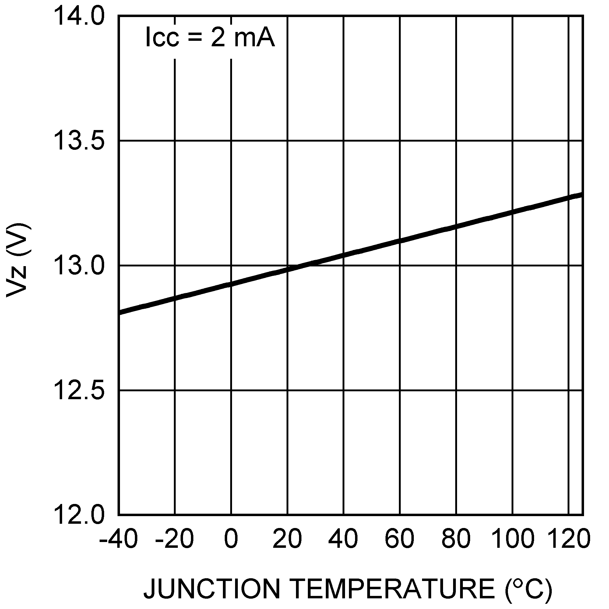 Figure 7-12 VZ Operating Voltage vs Temperature
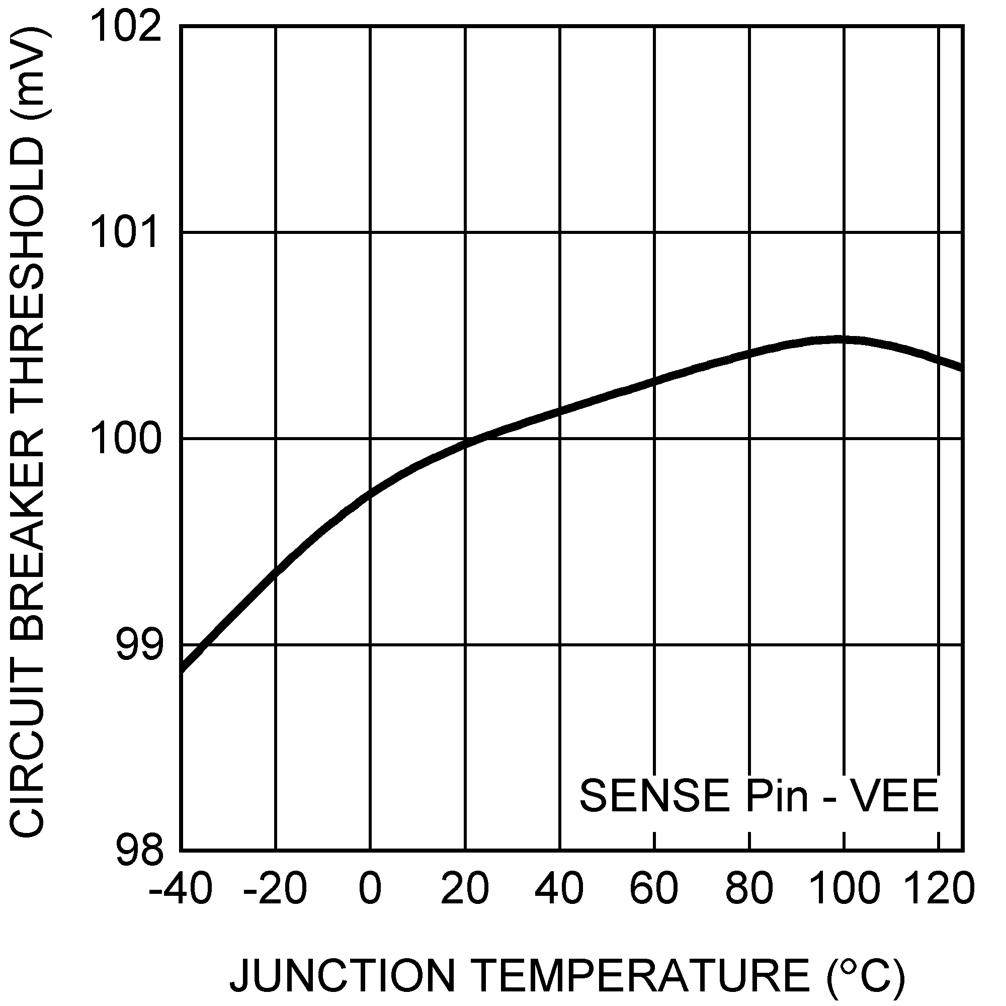 Figure 7-14 Circuit Breaker Threshold vs Temperature
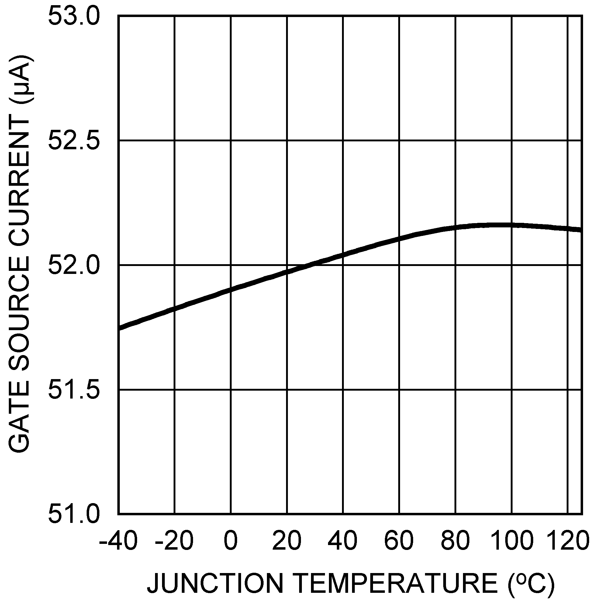 Figure 7-16 Gate Source Current vs Temperature
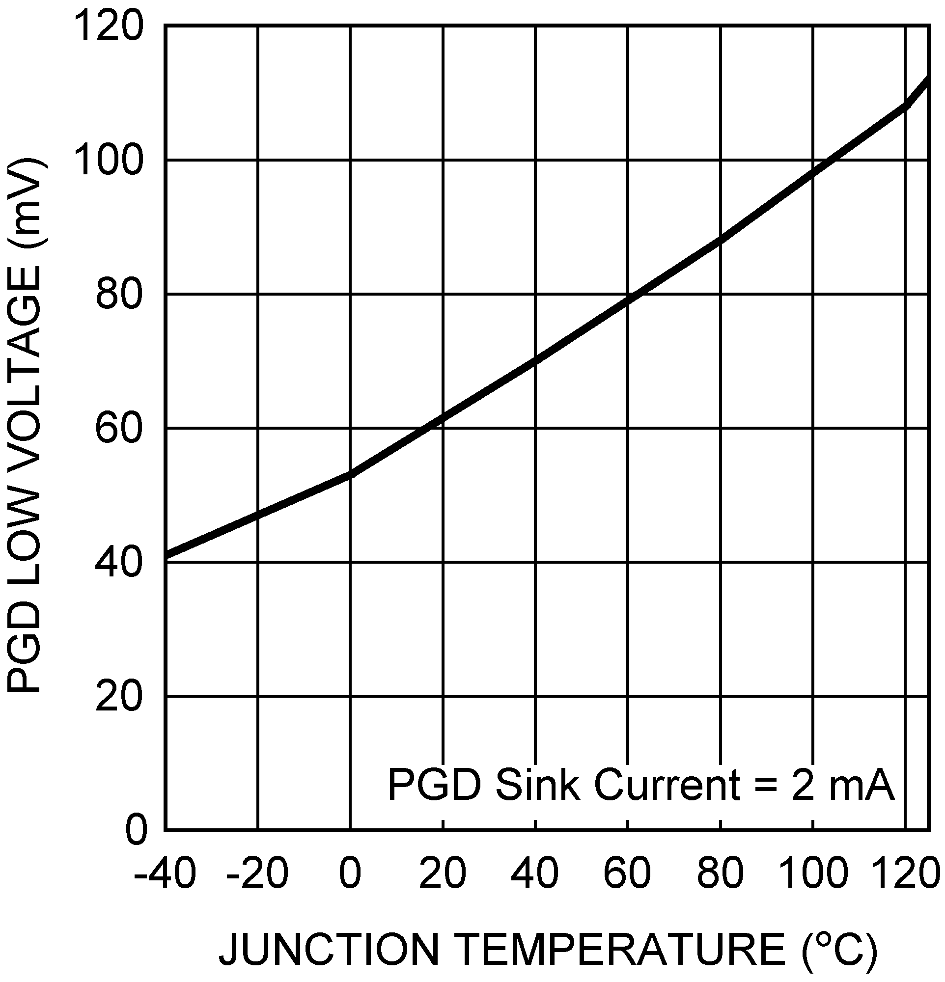 Figure 7-18 PGD Pin Low Voltage vs Temperature
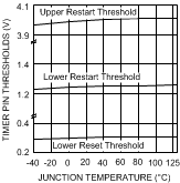 Figure 7-20 TIMER Pin Thresholds vs Temperature