JAJSGX1G September 2006 – Jaunuary 2020 LM5069
PRODUCTION DATA.
- 1 特長
- 2 アプリケーション
- 3 概要
- 4 改訂履歴
- 5 Pin Configuration and Functions
- 6 Specifications
- 7 Detailed Description
-
8 Application and Implementation
- 8.1 Application Information
- 8.2
Typical Application
- 8.2.1
48-V, 10-A Hot Swap Design
- 8.2.1.1 Design Requirements
- 8.2.1.2 Detailed Design Procedure
- 8.2.1.3 Application Curves
- 8.2.1
48-V, 10-A Hot Swap Design
- 9 Power Supply Recommendations
- 10Layout
- 11デバイスおよびドキュメントのサポート
- 12メカニカル、パッケージ、および注文情報
7.4.2 Gate Control
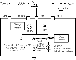
A charge pump provides internal bias voltage above the output voltage (OUT pin) to enhance the N-Channel MOSFET’s gate. The gate-to-source voltage is limited by an internal 12-V Zener diode. During normal operating conditions (t3 in Figure 22) the gate of Q1 is held charged by an internal 16-µA current source to approximately 12 V above OUT. If the maximum VGS rating of Q1 is less than 12 V, an external Zener diode of lower voltage must be added between the GATE and OUT pins. The external Zener diode must have a forward current rating of at least 250 mA.
When the system voltage is initially applied, the GATE pin is held low by a 230-mA pulldown current. This helps prevent an inadvertent turnon of the MOSFET through its drain-gate capacitance as the applied system voltage increases.
During the insertion time (t1 in Figure 22) the GATE pin is held low by a 2-mA pulldown current. This maintains Q1 in the off-state until the end of t1, regardless of the voltage at VIN or UVLO.
Following the insertion time, during t2 in Figure 22, the gate voltage of Q1 is modulated to keep the current or power dissipation level from exceeding the programmed levels. While in the current or power limiting mode the TIMER pin capacitor is charging. If the current and power limiting cease before the TIMER pin reaches 4 V the TIMER pin capacitor then discharges, and the circuit enters normal operation.
If the in-rush limiting condition persists such that the TIMER pin reached 4 V during t2, the GATE pin is then pulled low by the 2-mA pulldown current. The GATE pin is then held low until either a power-up sequence is initiated (LM5069-1), or until the end of the restart sequence (LM5069-2). See Fault Timer and Restart.
If the system input voltage falls below the UVLO threshold, or rises above the OVLO threshold, the GATE pin is pulled low by the 2-mA pulldown current to switch off Q1.
 Figure 23. Gate Control