JAJSGX1G September 2006 – Jaunuary 2020 LM5069
PRODUCTION DATA.
- 1 特長
- 2 アプリケーション
- 3 概要
- 4 改訂履歴
- 5 Pin Configuration and Functions
- 6 Specifications
- 7 Detailed Description
-
8 Application and Implementation
- 8.1 Application Information
- 8.2
Typical Application
- 8.2.1
48-V, 10-A Hot Swap Design
- 8.2.1.1 Design Requirements
- 8.2.1.2 Detailed Design Procedure
- 8.2.1.3 Application Curves
- 8.2.1
48-V, 10-A Hot Swap Design
- 9 Power Supply Recommendations
- 10Layout
- 11デバイスおよびドキュメントのサポート
- 12メカニカル、パッケージ、および注文情報
7.4.3 Fault Timer and Restart
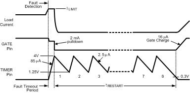
When the current limit or power limit threshold is reached during turnon or as a result of a fault condition, the gate-to-source voltage of Q1 is modulated to regulate the load current and power dissipation. When either limiting function is activated, an 85-µA fault timer current source charges the external capacitor (CT) at the TIMER pin as shown in Figure 25 (fault timeout period). If the fault condition subsides during the fault timeout period before the TIMER pin reaches 4 V, the LM5069 returns to the normal operating mode and CT is discharged by the 2.5-µA current sink. If the TIMER pin reaches 4 V during the fault timeout period, Q1 is switched off by a 2-mA pulldown current at the GATE pin. The subsequent restart procedure then depends on which version of the LM5069 is in use.
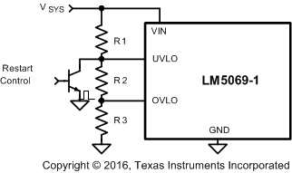
The LM5069-1 latches the GATE pin low at the end of the fault timeout period. CT is then discharged to ground by the 2.5-µA fault current sink. The GATE pin is held low by the 2-mA pulldown current until a power-up sequence is externally initiated by cycling the input voltage (VSYS), or momentarily pulling the UVLO pin below 2.5 V with an open-collector or open-drain device as shown in Figure 24. The voltage at the TIMER pin must be <0.3 V for the restart procedure to be effective.
 Figure 24. Latched Fault Restart Control
 The LM5069-2 provides an automatic restart sequence which consists of the TIMER pin cycling between 4 V and 1.25 V seven times after the fault timeout period, as shown in Figure 25. The period of each cycle is determined by the 85-µA charging current, and the 2.5-µA discharge current, and the value of the capacitor CT. When the TIMER pin reaches 0.3 V during the eighth high-to-low ramp, the 16-µA current source at the GATE pin turns on Q1. If the fault condition is still present, the fault timeout period and the restart cycle repeat.
 Figure 25. Restart Sequence (LM5069-2)