JAJSGX1G September 2006 – Jaunuary 2020 LM5069
PRODUCTION DATA.
- 1 特長
- 2 アプリケーション
- 3 概要
- 4 改訂履歴
- 5 Pin Configuration and Functions
- 6 Specifications
- 7 Detailed Description
-
8 Application and Implementation
- 8.1 Application Information
- 8.2
Typical Application
- 8.2.1
48-V, 10-A Hot Swap Design
- 8.2.1.1 Design Requirements
- 8.2.1.2 Detailed Design Procedure
- 8.2.1.3 Application Curves
- 8.2.1
48-V, 10-A Hot Swap Design
- 9 Power Supply Recommendations
- 10Layout
- 11デバイスおよびドキュメントのサポート
- 12メカニカル、パッケージ、および注文情報
8.2.1.2.1 Select RSNS and CL setting
The LM5069 monitors the current in the external MOSFET (Q1) by measuring the voltage across the sense resistor (RS), connected from VIN to SENSE. When the voltage difference across the VIN and SENSE pins (VCL) is greater than 55 mV (typical), the LM5069 begins modulating the MOSFET gate. Size RSNS for maximum or minimum VCL for applications that require ensured shutoff or ensured conduction. RSNS is sized to exhibit minimum VCL across RSNS at maximum load current in Equation 1.

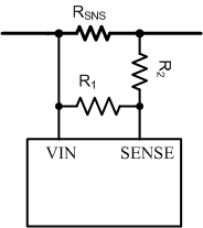
Typically sense resistors are only available in discrete value. We choose the next smallest discrete value, 4 mΩ. If a precise current limit is desired, a sense resistor along with a resistor divider can be used as shown in Figure 29.
 Figure 29. SENSE Resistor Divider
 If using a resistor divider, then the next larger available sense resistor must be chosen (5 mΩ in this example). The ratio of R1 and R2 can then be calculated with Equation 2.

Note that the SENSE pin pulls 23 µA of current, which creates an offset across R2. TI recommends keeping R2 below 10 Ω to reduce the offset that this introduces. In addition, the 1% resistors add to the current monitoring error. Finally, if the resistor divider approach is used, compute the effective sense resistance (RSNS, EFF) using Equation 3 and use that in all equations instead of RSNS.

Note that for many applications, a precise current limit may not be required. In that case, it’s simpler to pick the next smaller available sense resistor.