SNOSAW2Q September 2006 – November 2015 LM5100A , LM5100B , LM5100C , LM5101A , LM5101B , LM5101C
PRODUCTION DATA.
- 1 Features
- 2 Applications
- 3 Description
- 4 Revision History
- 5 Device Comparison Table
- 6 Pin Configuration and Functions
- 7 Specifications
- 8 Detailed Description
- 9 Application and Implementation
- 10Power Supply Recommendations
- 11Layout
- 12Device and Documentation Support
- 13Mechanical, Packaging, and Orderable Information
パッケージ・オプション
メカニカル・データ(パッケージ|ピン)
サーマルパッド・メカニカル・データ
発注情報
6 Pin Configuration and Functions
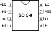
D Package
8-Pin SOIC
Top View
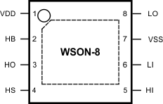
NGT Package
8-Pin WSON With Exposed Thermal Pad
Top View
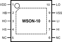
DPR Package
10-Pin WSON With Exposed Thermal Pad
Top View
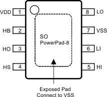
DDA Package
8-Pin SO PowerPAD
Top View
DGN Package
8-Pin MSOP-PowerPAD
Top View
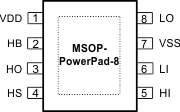
Pin Functions
| PIN | I/O | DESCRIPTION | ||||
|---|---|---|---|---|---|---|
| NAME | 8 PINS | 10 PINS(1) | ||||
| HB | 2 | 2 | I | High-side gate driver bootstrap supply. Connect the positive terminal of the bootstrap capacitor to HB and the negative terminal to HS. The bootstrap capacitor should be placed as close to the IC as possible. | ||
| HI | 5 | 7 | I | High-side driver control input. The LM5100A/B/C inputs have CMOS type thresholds. The LM5101A/B/C inputs have TTL type thresholds. Unused inputs should be tied to ground and not left open. | ||
| HO | 3 | 3 | O | High-side gate driver output. Connect to the gate of high-side MOSFET with a short, low inductance path. | ||
| HS | 4 | 4 | — | High-side MOSFET source connection. Connect to the bootstrap capacitor negative terminal and the source of the high-side MOSFET. | ||
| LI | 6 | 8 | I | Low-side driver control input. The LM5100A/B/C inputs have CMOS type thresholds. The LM5101A/B/C inputs have TTL type thresholds. Unused inputs should be tied to ground and not left open. | ||
| LO | 8 | 10 | O | Low-side gate driver output. Connect to the gate of the low-side MOSFET with a short, low inductance path. | ||
| VDD | 1 | 1 | I | Positive gate drive supply . Locally decouple to VSS using low ESR/ESL capacitor located as close to the IC as possible. | ||
| VSS | 7 | 9 | — | Ground return. All signals are referenced to this ground. | ||
| EP(2) | — | TI recommends that the exposed pad on the bottom of the package is soldered to ground plane on the PC board, and that ground plane should extend out from beneath the IC to help dissipate heat. | ||||
(1) For WSON-10 package, pins 5 and 6 have no connection.
(2) Exposed pad is not available on the 8-pin SOIC package.