JAJSC49E February 2005 – August 2016 LM5105
PRODUCTION DATA.
8 Application and Implementation
NOTE
Information in the following applications sections is not part of the TI component specification, and TI does not warrant its accuracy or completeness. TI’s customers are responsible for determining suitability of components for their purposes. Customers should validate and test their design implementation to confirm system functionality.
8.1 Application Information
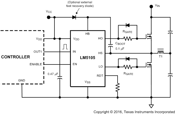
The LM5105 is one of the latest generation of high-voltage gate drivers which are designed to drive both the high-side and low-side N-channel MOSFETs in a half-bridge or full-bridge configuration or in a synchronous buck circuit. The floating high-side driver can operate with supply voltages up to 110 V. This allows for N-channel MOSFET control in half-bridge, full-bridge, push-pull, two-switch forward, and active clamp topologies.
The outputs of the LM5105 are controlled from a single input. The rising edge of each output can be delayed with a programming resistor.
8.2 Typical Application
 Figure 20. LM5105 Driving MOSFETS Connected in Half-Bridge Configuration
8.2.1 Design Requirements
Table 2 lists the design parameters for this application example.
Table 2. Design Parameters
| PARAMETER | VALUE |
|---|---|
| Gate Drive IC | LM5105 |
| Mosfet | CSD18531Q5A |
| VDD | 10 V |
| Qgmax | 43 nC |
| Fsw | 100 kHz |
| DMax | 95% |
| IHBS | 10 µA |
| VDH | 1.1 V |
| VHBR | 7.1 V |
| VHBH | 0.4 V |
8.2.2 Detailed Design Procedure
where
- VDD = Supply voltage of the gate drive IC
- VDH = Bootstrap diode forward voltage drop
- Vgsmin = Minimum gate source threshold voltage


The quiescent current of the bootstrap circuit is 10 µA, which is negligible compared to the Qgs of the MOSFET.

In practice the value for the CBOOT capacitor should be greater than that calculated to allow for situations where the power stage may skip pulse due to load transients. In this circumstance the boot capacitor must maintain the HB pin voltage above the UVLO voltage for the HB circuit.
As a general rule the local VDD bypass capacitor should be 10 times greater than the calculated value of CBOOT.
In practice, the value of CBoot is greater than the calculated value. This allows for the capacitance shift caused by the DC bias voltage and for situations where the power stage would otherwise skip pulses due to load transients. Therefore, it is recommended to include a safety-related margin in the CBoot value and place it as close to the VDD and VSS pins as possible. A 50-V, 0.1-µF capacitor is chosen in this example.
The bootstrap and bias capacitors should be ceramic types with X7R dielectric. The voltage rating should be twice that of the maximum VDD to allow for loss of capacitance once the devices have a DC bias voltage across them and to ensure long-term reliability of the devices.
The resistor values, RT, for setting turnon delay can be found in Figure 17.
8.2.3 Application Curves
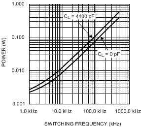
 Figure 21. Diode Power Dissipation, VIN = 80 V
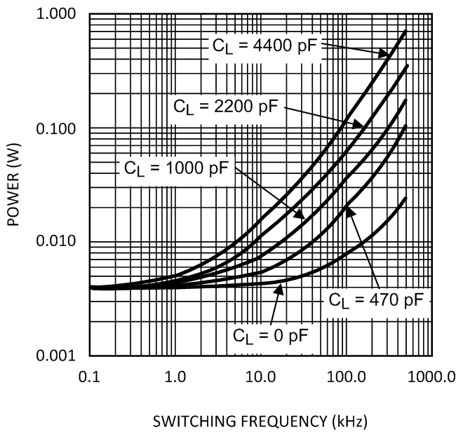
 Figure 23. Gate Driver Power Dissipation (LO + HO)
VCC = 12 V, Neglecting Diode Losses
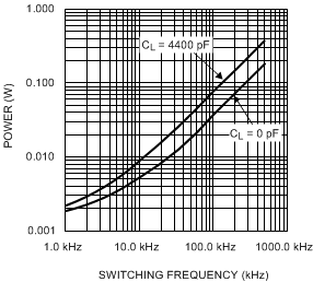
 Figure 22. Diode Power Dissipation, VIN = 40 V