JAJSC58H July 2004 – September 2016 LM5111
PRODUCTION DATA.
- 1 特長
- 2 アプリケーション
- 3 概要
- 4 改訂履歴
- 5 デバイスのオプション
- 6 Pin Configuration and Functions
- 7 Specifications
- 8 Detailed Description
- 9 Application and Implementation
- 10Power Supply Recommendations
- 11Layout
- 12デバイスおよびドキュメントのサポート
- 13メカニカル、パッケージ、および注文情報
パッケージ・オプション
メカニカル・データ(パッケージ|ピン)
サーマルパッド・メカニカル・データ
- DGN|8
発注情報
9 Application and Implementation
NOTE
Information in the following applications sections is not part of the TI component specification, and TI does not warrant its accuracy or completeness. TI’s customers are responsible for determining suitability of components for their purposes. Customers should validate and test their design implementation to confirm system functionality.
9.1 Application Information
High-frequency power supplies often require high-speed, high-current drivers such as the LM5111 family. A leading application is the need to provide a high-power buffer stage between the PWM output of the control IC and the gates of the primary power MOSFET or IGBT switching devices. In other cases, the driver IC is used to drive the power-device gates through a drive transformer. Synchronous rectification supplies are also needed to simultaneously drive multiple devices which presents an extremely large load to the control circuitry.
Driver ICs are used when use of the primary PWM regulator IC to directly drive the switching devices for one or more reasons is not feasible. The PWMIC does not have the brute drive capability required for the intended switching MOSFET, limiting the switching performance in the application. In other cases, there may be a desire to minimize the effect of high-frequency switching noise by placing the high current driver physically close to the load. Also, newer ICs that target the highest operating frequencies do not incorporate onboard gate drivers at all. Their PWM outputs are only intended to drive the high impedance input to a driver such as the UCCx732x. Finally, the control IC is under thermal stress due to power dissipation, and an external driver helps by moving the heat from the controller to an external package.
9.2 Typical Application
 Figure 12. LM5111 Driving Two Independent MOSFETs
9.2.1 Design Requirements
To select the proper device from the LM5111 family, TI recommends first checking the appropriate logic for the outputs. LM5111 has dual inverting outputs; dual noninverting outputs; inverting channel A and noninverting channel B. Refer to operating modes to select which driver from the family is required in a given application. Moreover, some design considerations must be evaluated first in order to make the most appropriate selection. Among these considerations are VCC and power dissipation.
9.2.2 Detailed Design Procedure
9.2.2.1 VCC
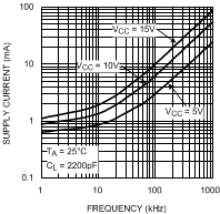
Although quiescent VCC current is very low, total supply current will be higher, depending on OUTA and OUTB current and the programmed oscillator frequency. Total VCC current is the sum of quiescent VCC current and the average OUT current. Knowing the operating frequency and the MOSFET gate charge (Qg), average OUT current can be calculated using Equation 1.
where
- f is frequency
For the best high-speed circuit performance, two VCC bypass capacitors are recommended to prevent noise problems. The use of surface mount components is highly recommended. A 0.1-µF ceramic capacitor should be located closest to the VDD to ground connection. In addition, a larger capacitor (such as 1 µF and above) with relatively low ESR should be connected in parallel, to help deliver the high current peaks to the load. The parallel combination of capacitors should present a low impedance characteristic for the expected current levels in the driver application.
9.2.3 Application Curves

