JAJSC47I June 2011 – October 2019 LM5113
PRODUCTION DATA.
- 1 特長
- 2 アプリケーション
- 3 概要
- 4 改訂履歴
- 5 概要(続き)
- 6 Pin Configuration and Functions
- 7 Specifications
- 8 Detailed Description
- 9 Application and Implementation
- 10Power Supply Recommendations
- 11Layout
- 12デバイスおよびドキュメントのサポート
- 13メカニカル、パッケージ、および注文情報
パッケージ・オプション
メカニカル・データ(パッケージ|ピン)
サーマルパッド・メカニカル・データ
発注情報
8.3.1 Input and Output
The inputs are independently controlled with TTL input thresholds, and can withstand voltages up to 14 V regardless of the VDD voltage, which means it could be directly connected to the outputs of PWM controllers with up to 14-V power supply, saving a buffer stage between output of higher-voltage powered controller, for example LM5025 with 10 V, and input of the LM5113.
The output pulldown and pullup resistance of LM5113 is optimized for enhancement mode GaN FETs to achieve high frequency and efficient operation. The 0.6-Ω pulldown resistance provides a robust low impedance turnoff path necessary to eliminate undesired turnon induced by high dv/dt or high di/dt. The 2.1-Ω pullup resistance helps reduce the ringing and over-shoot of the switch node voltage. The split outputs of the LM5113 offer flexibility to adjust the turnon and turnoff speed by independently adding additional impedance in either the turnon path, the turnoff path, or both.
It is very important that the input signal of the two channels HI and LI, which has logic compatible threshold and hysteresis, must be tied to either VDD or VSS if they are not used. This inputs must not be left floating.
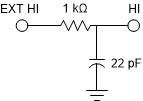
Additionally, the input signals avoid pulses shorter than 3 ns by using the input filter to the HI and LI input pins. The values and part numbers of the circuit components are shown in the Figure 16.
 Figure 16. Input Filter 1 (High-Side Input Filter)
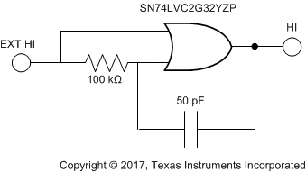
 If short pulses or short delays are required, the circuit in Figure 17 is recommended.
 Figure 17. Input Filter 1 for Short Pulses (High-Side Input Filter)