JAJSDG9 June 2017 LM5118-Q1
PRODUCTION DATA.
- 1 特長
- 2 アプリケーション
- 3 概要
- 4 改訂履歴
- 5 Pin Configuration and Functions
- 6 Specifications
- 7 Detailed Description
-
8 Application and Implementation
- 8.1 Application Information
- 8.2
Typical Application
- 8.2.1 Design Requirements
- 8.2.2
Detailed Design Procedure
- 8.2.2.1 Custom Design With WEBENCH® Tools
- 8.2.2.2 R7 = RT
- 8.2.2.3 Inductor Selection, L1
- 8.2.2.4 R13 = RSENSE
- 8.2.2.5 C15 = CRAMP
- 8.2.2.6 Inductor Current Limit Calculation
- 8.2.2.7 C9 - C12 = Output Capacitors
- 8.2.2.8 D1
- 8.2.2.9 D4
- 8.2.2.10 C1 - C5 = Input Capacitor
- 8.2.2.11 C20
- 8.2.2.12 C8
- 8.2.2.13 C16 = CSS
- 8.2.2.14 R8, R9
- 8.2.2.15 R1, R3, C21
- 8.2.2.16 R2
- 8.2.2.17 Snubber
- 8.2.2.18 Error Amplifier Configuration
- 8.2.3 Application Curves
- 9 Power Supply Recommendations
- 10Layout
- 11デバイスおよびドキュメントのサポート
- 12メカニカル、パッケージ、および注文情報
7 Detailed Description
7.1 Overview
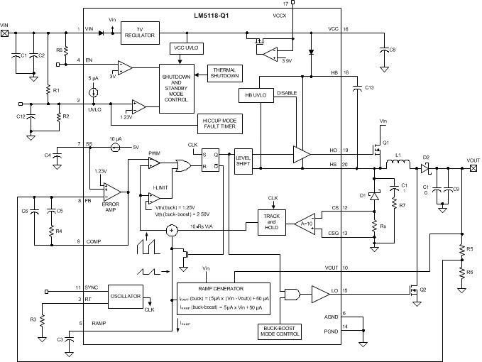
The LM5118-Q1 high voltage switching regulator features all of the functions necessary to implement an efficient high voltage buck or buck-boost regulator using a minimum of external components. The regulator switches smoothly from buck to buck-boost operation as the input voltage approaches the output voltage, allowing operation with the input greater than or less than the output voltage. This easy to use regulator integrates high-side and low-side MOSFET drivers capable of supplying peak currents of 2 A. The regulator control method is based on current mode control using an emulated current ramp. Peak current mode control provides inherent line feed-forward, cycle-by-cycle current limiting and ease of loop compensation. The use of an emulated control ramp reduces noise sensitivity of the pulse-width modulation circuit, allowing reliable processing of very small duty cycles necessary in high input voltage applications. The operating frequency is user programmable from 50 kHz to 500 kHz. An oscillator synchronization pin allows multiple LM5118-Q1 regulators to self synchronize or be synchronized to an external clock. Fault protection features include current limiting, thermal shutdown, and remote shutdown capability. An undervoltage lockout input allows regulator shutdown when the input voltage is below a user selected threshold, and a low state at the enable pin will put the regulator into an extremely low current shutdown state. The device is available in the HTSSOP-20EP package featuring an exposed pad to aid in thermal dissipation.
7.2 Functional Block Diagram
7.3 Feature Description
A buck-boost regulator can maintain regulation for input voltages either higher or lower than the output voltage. The challenge is that buck-boost power converters are not as efficient as buck regulators. The LM5118-Q1 has been designed as a dual-mode controller whereby the power converter acts as a buck regulator while the input voltage is above the output. As the input voltage approaches the output voltage, a gradual transition to the buck-boost mode occurs. The dual-mode approach maintains regulation over a wide range of input voltages, while maintaining the optimal conversion efficiency in the normal buck mode. The gradual transition between modes eliminates disturbances at the output during transitions. Figure 8 shows the basic operation of the LM5118-Q1 regulator in the buck mode. In buck mode, transistor Q1 is active and Q2 is disabled. The inductor current ramps in proportion to the VIN – VOUT voltage difference when Q1 is active and ramps down through the recirculating diode D1 when Q1 is off. The first order buck mode transfer function is VOUT/VIN = D, where D is the duty cycle of the buck switch, Q1.
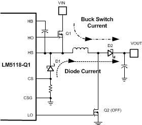 Figure 8. Buck Mode Operation
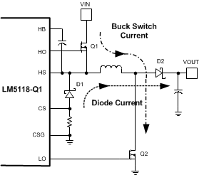
Figure 9 shows the basic operation of buck-boost mode. In buck-boost mode both Q1 and Q2 are active for the same time interval each cycle. The inductor current ramps up (proportional to VIN) when Q1 and Q2 are active and ramps down through the recirculating diode during the off time. The first order buck-boost transfer function is VOUT/VIN = D/(1-D), where D is the duty cycle of Q1 and Q2.
7.3.1 UVLO
An undervoltage lockout pin is provided to disable the regulator when the input is below the desired operating range. If the UVLO pin is below 1.13 V, the regulator enters a standby mode with the outputs disabled, but with VCC regulator operating. If the UVLO input exceeds 1.23 V, the regulator will resume normal operation. A voltage divider from the input to ground can be used to set a VIN threshold to disable the regulator in brownout conditions or for low input faults.
If a current limit fault exists for more than 256 clock cycles, the regulator will enter a hiccup mode of current limiting and the UVLO pin will be pulled low by an internal switch. This switch turns off when the UVLO pin approaches ground potential allowing the UVLO pin to rise. A capacitor connected to the UVLO pin will delay the return to a normal operating level and thereby set the off-time of the hiccup mode fault protection. An internal 5-µA pullup current pulls the UVLO pin to a high state to ensure normal operation when the VIN UVLO function is not required and the pin is left floating.
7.3.2 Oscillator and Sync Capability
The LM5118-Q1 oscillator frequency is set by a single external resistor connected between the RT pin and the AGND pin. The RT resistor should be located very close to the device and connected directly to the pins of the IC. To set a desired oscillator frequency (f), the necessary value for the RT resistor can be calculated from Equation 1:

The SYNC pin can be used to synchronize the internal oscillator to an external clock. The external clock must be of higher frequency than the free-running frequency set by the RT resistor. A clock circuit with an open-drain output is the recommended interface from the external clock to the SYNC pin. The clock pulse duration should be greater than 15 ns.
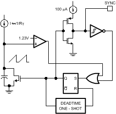
Multiple LM5118-Q1 devices can be synchronized together simply by connecting the SYNC pins together as in Figure 11. In this configuration, all of the devices are synchronized to the highest frequency device. Figure 12 shows the SYNC input and output features of the LM5118-Q1. The internal oscillator circuit drives the SYNC pin with a strong pull down or weak pullup inverter. When the SYNC pin is pulled low, either by the internal oscillator or an external clock, the ramp cycle of the oscillator is terminated and forced 400 ns off-time is initiated before a new oscillator cycle begins. If the SYNC pins of several LM5118-Q1 IC’s are connected together, the IC with the highest internal clock frequency will pull all the connected SYNC pins low and terminate the oscillator ramp cycles of the other ICs. The LM5118-Q1 with the highest programmed clock frequency will serve as the master and control the switching frequency of all the devices with lower oscillator frequencies.
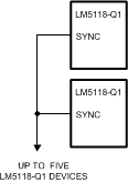 Figure 11. Sync From Multiple Devices
7.3.3 Error Amplifier and PWM Comparator
The internal high gain error amplifier generates an error signal proportional to the difference between the regulated output voltage and an internal precision reference (1.23 V). The output of the error amplifier is connected to the COMP pin. Loop compensation components, typically a type II network shown in are connected between the COMP and FB pins. This network creates a low frequency pole, a zero, and a noise reducing high frequency pole. The PWM comparator compares the emulated current sense signal from the RAMP generator to the error amplifier output voltage at the COMP pin. The same error amplifier is used for operation in buck and buck-boost mode.
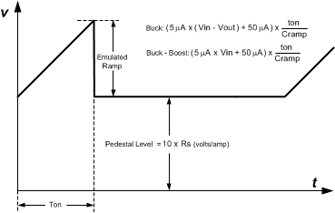 Figure 13. Composition of Emulated Current Signal
7.3.4 Ramp Generator
The ramp signal of a pulse-width modulator with current mode control is typically derived directly from the buck switch drain current. This switch current corresponds to the positive slope portion of the inductor current signal. Using this signal for the PWM ramp simplifies the control loop transfer function to a single pole response and provides inherent input voltage feed-forward compensation. The disadvantage of using the buck switch current signal for PWM control is the large leading edge spike due to circuit parasitics. The leading edge spike must be filtered or blanked to avoid early termination of the PWM pulse. Also, the current measurement may introduce significant propagation delays. The filtering, blanking time and propagation delay limit the minimal achievable pulse width. In applications where the input voltage may be relatively large in comparison to the output voltage, controlling a small pulse width is necessary for regulation. The LM5118-Q1 uses a unique ramp generator which does not actually measure the buck switch current but instead creates a signal representing or emulating the inductor current. The emulated ramp provides signal to the PWM comparator that is free of leading edge spikes and measurement or filtering delays. The current reconstruction is comprised of two elements, a sample-and-hold pedestal level and a ramp capacitor which is charged by a controlled current source. Refer to Figure 13 for details.
The sample-and-hold pedestal level is derived from a measurement of the recirculating current through a current sense resistor in series with the recirculating diode of the buck regulator stage. A small value current sensing resistor is required between the recirculating diode anode and ground. The CS and CSG pins should be Kelvin connected directly to the sense resistor. The voltage level across the sense resistor is sampled and held just prior to the onset of the next conduction interval of the buck switch. The current sensing and sample-and-hold provide the DC level of the reconstructed current signal. The sample and hold of the recirculating diode current is valid for both buck and buck-boost modes. The positive slope inductor current ramp is emulated by an external capacitor connected from the RAMP pin to the AGND and an internal voltage controlled current source. In buck mode, the ramp current source that emulates the inductor current is a function of the VIN and VOUT voltages per Equation 2:

In buck-boost mode, the ramp current source is a function of the input voltage VIN, per Equation 3:

Proper selection of the RAMP capacitor (CRAMP) depends upon the value of the output inductor (L) and the current sense resistor (RS). For proper current emulation, the sample and hold pedestal value and the ramp amplitude must have the same relative relationship to the actual inductor current. That is:

where
- gm is the ramp generator transconductance (5 µA/V)
- A is the current sense amplifier gain (10V/V)
The ramp capacitor should be located very close to the device and connected directly to the RAMP and AGND pins.
The relationship between the average inductor current and the pedestal value of the sampled inductor current can cause instability in certain operating conditions. This instability is known as sub-harmonic oscillation, which occurs when the inductor ripple current does not return to its initial value by the start of the next switching cycle. Sub-harmonic oscillation is normally characterized by observing alternating wide and narrow pulses at the switch node. Adding a fixed slope voltage ramp (slope compensation) to the current sense signal prevents this oscillation. The 50 µA of offset current provided from the emulated current source adds enough slope compensation to the ramp signal for output voltages less than or equal to 12 V. For higher output voltages, additional slope compensation may be required. In such applications, the ramp capacitor can be decreased from the nominal calculated value to increase the ramp slope compensation.
The pedestal current sample is obtained from the current sense resistor (Rs) connected to the CS and CSG pins. It is sometimes helpful to adjust the internal current sense amplifier gain (A) to a lower value in order to obtain the higher current limit threshold. Adding a pair of external resistors RG in a series with CS and CSG as in Figure 14 reduces the current sense amplifier gain A according to Equation 5:

7.3.5 Current Limit
In the buck mode the average inductor current is equal to the output current (IOUT). In buck-boost mode the average inductor current is approximately equal to:

Consequently, the inductor current in buck-boost mode is much larger especially when VOUT is large relative to VIN. The LM5118-Q1 provides a current monitoring scheme to protect the circuit from possible over-current conditions. When set correctly, the emulated current sense signal is proportional to the buck switch current with a scale factor determined by the current sense resistor. The emulated ramp signal is applied to the current limit comparator. If the peak of the emulated ramp signal exceeds 1.25 V when operating in the buck mode, the PWM cycle is immediately terminated (cycle-by-cycle current limiting). In buck-boost mode the current limit threshold is increased to 2.50 V to allow higher peak inductor current. To further protect the external switches during prolonged overload conditions, an internal counter detects consecutive cycles of current limiting. If the counter detects 256 consecutive current limited PWM cycles, the LM5118-Q1 enters a low power dissipation hiccup mode. In the hiccup mode, the output drivers are disabled, the UVLO pin is momentarily pulled low, and the soft-start capacitor is discharged. The regulator is restarted with a normal soft-start sequence once the UVLO pin charges back to 1.23 V. The hiccup mode off-time can be programmed by an external capacitor connected from UVLO pin to ground. This hiccup cycle will repeat until the output overload condition is removed.
In applications with low output inductance and high input voltage, the switch current may overshoot due to the propagation delay of the current limit comparator and control circuitry. If an overshoot should occur, the sample-and-hold circuit will detect the excess recirculating diode current. If the sample-and-hold pedestal level exceeds the internal current limit threshold, the buck switch will be disabled and will skip PWM cycles until the inductor current has decayed below the current limit threshold. This approach prevents current runaway conditions due to propagation delays or inductor saturation since the inductor current is forced to decay before the buck switch is turned on again.
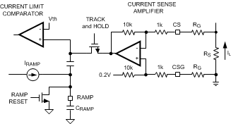 Figure 14. Current Limit and Ramp Circuit
7.3.6 Maximum Duty Cycle
Each conduction cycle of the buck switch is followed by a forced minimum off-time of 400 ns to allow sufficient time for the recirculating diode current to be sampled. This forced off-time limits the maximum duty cycle of the controller. The actual maximum duty cycle will vary with the operating frequency as follows:
where
- f is the oscillator frequency in Hz
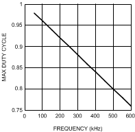 Figure 15. Maximum Duty Cycle vs Frequency
Limiting the maximum duty cycle will limit the maximum boost ratio (VOUT/VIN) while operating in buck-boost mode. For example, from Figure 15, at an operating frequency of 500 kHz, DMAX is 80%. Using the buck-boost transfer function.

With D = 80%, solving for VOUT results in:
With a minimum input voltage of 5 V, the maximum possible output voltage is 20 V at f = 500 kHz. The buck-boost step-up ratio can be increased by reducing the operating frequency which increases the maximum duty cycle.
7.3.7 Soft Start
The soft-start feature allows the regulator to gradually reach the initial steady-state operating point, thus reducing start-up stresses and surges. The internal 10-µA soft-start current source gradually charges an external soft-start capacitor connected to the SS pin. The SS pin is connected to the positive input of the internal error amplifier. The error amplifier controls the pulse-width modulator such that the FB pin approximately equals the SS pin as the SS capacitor is charged. Once the SS pin voltage exceeds the internal 1.23-V reference voltage, the error amp is controlled by the reference instead of the SS pin. The SS pin voltage is clamped by an internal amplifier at a level of 150 mV above the FB pin voltage. This feature provides a soft-start controlled recovery in the event a severe overload pulls the output voltage (and FB pin) well below normal regulation but does not persist for 256 clock cycles.
Various sequencing and tracking schemes can be implemented using external circuits that limit or clamp the voltage level of the SS pin. The SS pin acts as a non-inverting input to the error amplifier anytime SS voltage is less than the 1.23-V reference. In the event a fault is detected (overtemperature, VCC undervoltage, hiccup current limit), the soft-start capacitor will be discharged. When the fault condition is no longer present, a new soft-start sequence will begin.
7.3.8 HO Output
The LM5118-Q1 contains a high-side, high-current gate driver and associated high voltage level shift. This gate driver circuit works in conjunction with an internal diode and an external bootstrap capacitor. A 0.1-µF ceramic capacitor, connected with short traces between the HB pin and HS pin is recommended for most circuit configurations. The size of the bootstrap capacitor depends on the gate charge of the external FET. During the off time of the buck switch, the HS pin voltage is approximately –0.5 V and the bootstrap capacitor is charged from VCC through the internal bootstrap diode. When operating with a high PWM duty cycle, the buck switch will be forced off each cycle for 400 ns to ensure that the bootstrap capacitor is recharged.
7.3.9 Thermal Protection
Internal Thermal Shutdown circuitry is provided to protect the integrated circuit in the event the maximum junction temperature is exceeded. When activated, typically at 165°C, the controller is forced into a low power reset state, disabling the output driver and the bias regulator. This protection is provided to prevent catastrophic failures from accidental device overheating.
7.4 Device Functional Modes
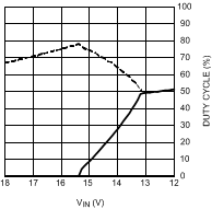
Figure 10 shows how duty cycle effects the operational mode and is useful for reference in the following discussions. Initially, only the buck switch is active and the buck duty cycle increases to maintain output regulation as VIN decreases. When VIN is approximately equal to 15.5 V, the boost switch begins to operate with a low duty cycle. If VIN continues to fall, the boost switch duty cycle increases and the buck switch duty cycle decreases until they become equal at VIN = 13.2 V.
7.4.1 Buck Mode Operation: VIN > VOUT
The LM5118-Q1 buck-boost regulator operates as a conventional buck regulator with emulated current mode control while VIN is greater than VOUT and the buck mode duty cycle is less than 75%. In buck mode, the LO gate drive output to the boost switch remains low.
7.4.2 Buck-Boost Mode Operation: VIN ≊ VOUT
When VIN decreases relative to VOUT, the duty cycle of the buck switch will increase to maintain regulation. Once the duty cycle reaches 75%, the boost switch starts to operate with a very small duty cycle. As VIN is further decreased, the boost switch duty cycle increases until it is the same as the buck switch. As VIN is further decreased below VOUT, the buck and boost switch operate together with the same duty cycle and the regulator is in full buck-boost mode. This feature allows the regulator to transition smoothly from buck to buck-boost mode. Note that the regulator can be designed to operate with VIN less than 4 V, but VIN must be at least 5 V Figure 16 presents a timing illustration of the gradual transition from buck to buck-boost mode when the input voltage ramps downward over a few switching cycles.
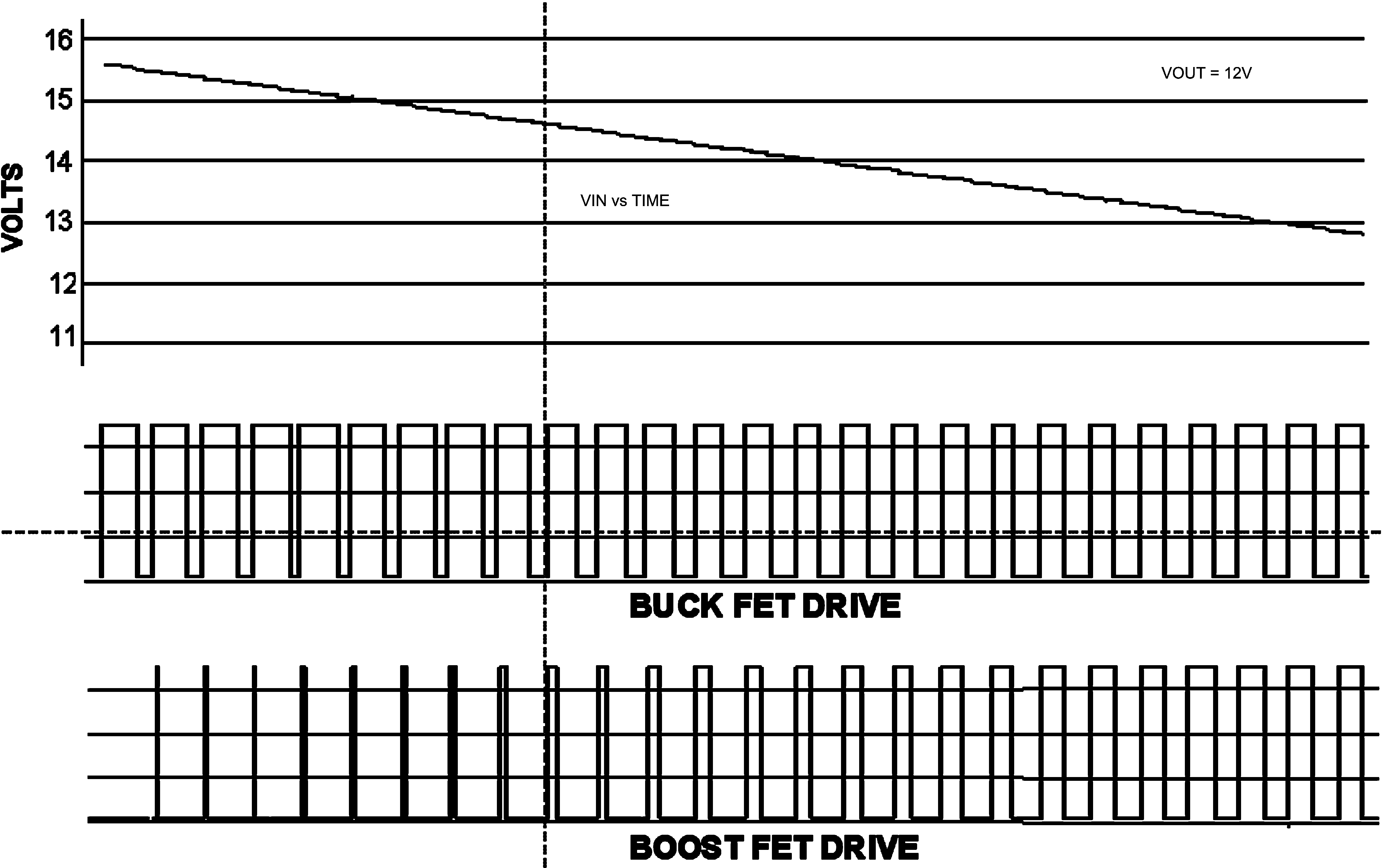 Figure 16. Buck (HO) and Boost (LO) Switch Duty Cycle vs. Time,
Illustrating Gradual Mode Change With Decreasing Input Voltage
7.4.3 High Voltage Start-Up Regulator
The LM5118-Q1 contains a dual-mode, high voltage linear regulator that provides the VCC bias supply for the PWM controller and the MOSFET gate driver. The VIN input pin can be connected directly to input voltages as high as 75 V. For input voltages below 10 V, an internal low dropout switch connects VCC directly to VIN. In this supply range, VCC is approximately equal to VIN. For VIN voltages greater than 10 V, the low dropout switch is disabled and the VCC regulator is enabled to maintain VCC at approximately 7 V. A wide operating range of 4 V to 75 V (with a start-up requirement of at least 5 V) is achieved through the use of this dual mode regulator.
The output of the VCC regulator is current limited to 35 mA, typical. Upon power up, the regulator sources current into the capacitor connected to the VCC pin. When the voltage at the VCC pin exceeds the VCC undervoltage threshold of 3.7 V and the UVLO input pin voltage is greater than 1.23 V, the gate driver outputs are enabled and a soft-start sequence begins. The gate driver outputs remain enabled until VCC falls below 3.5 V or the voltage at the UVLO pin falls below 1.13 V.
In many applications, the regulated output voltage or an auxiliary supply voltage can be applied to the VCCX pin to reduce the IC power dissipation. For output voltages between 4 V and 15 V, VOUT can be connected directly to VCCX. When the voltage at the VCCX pin is greater than 3.85 V, the internal VCC regulator is disabled and an internal switch connects VCCX to VCC, reducing the internal power dissipation.
In high voltage applications, take extrac care to ensure the VIN pin voltage does not exceed the absolute maximum voltage rating of 76 V. During line or load transients, voltage ringing on the VIN line that exceeds the absolute maximum rating can damage the IC. Both careful PCB layout and the use of quality bypass capacitors located close to the VIN and GND pins are essential.
 Figure 17. VIN and VCC Sequencing
7.4.4 Enable
The LM5118-Q1 contains an enable function which provides a very low input current shutdown mode. If the EN pin is pulled below 0.5 V, the regulator enters shutdown mode, drawing less than 10 µA from the VIN pin. Raising the EN input above 3 V returns the regulator to normal operation. The EN pin can be tied directly to the VIN pin if this function is not needed. It must not be left floating. A 1-MΩ pullup resistor to VIN can be used to interface with an open-collector or open-drain control signal.