JAJSNE2 October 2022 LM51231-Q1
PRODUCTION DATA
- 1 特長
- 2 アプリケーション
- 3 概要
- 4 Revision History
- 5 Pin Configuration and Functions
- 6 Specifications
-
7 Detailed Description
- 7.1 Overview
- 7.2 Functional Block Diagram
- 7.3
Feature Description
- 7.3.1 Device Enable/Disable (EN, VH Pin)
- 7.3.2 High Voltage VCC Regulator (BIAS, VCC Pin)
- 7.3.3 Light Load Switching Mode Selection (MODE Pin)
- 7.3.4 VOUT Range Selection (RANGE Pin)
- 7.3.5 Line Undervoltage Lockout (UVLO Pin)
- 7.3.6 Fast Restart using VCC HOLD (VH Pin)
- 7.3.7 Adjustable Output Regulation Target (VOUT, TRK, VREF Pin)
- 7.3.8 Overvoltage Protection (VOUT Pin)
- 7.3.9 Power Good Indicator (PGOOD Pin)
- 7.3.10 Dynamically Programmable Switching Frequency (RT)
- 7.3.11 External Clock Synchronization (SYNC Pin)
- 7.3.12 Programmable Spread Spectrum (DITHER Pin)
- 7.3.13 Programmable Soft-start (SS Pin)
- 7.3.14 Wide Bandwidth Transconductance Error Amplifier and PWM (TRK, COMP Pin)
- 7.3.15 Current Sensing and Slope Compensation (CSP, CSN Pin)
- 7.3.16 Constant Peak Current Limit (CSP, CSN Pin)
- 7.3.17 Maximum Duty Cycle and Minimum Controllable On-time Limits
- 7.3.18 MOSFET Drivers, Integrated Boot Diode, and Hiccup Mode Fault Protection (LO, HO, HB Pin)
- 7.3.19 Thermal Shutdown Protection
- 7.4 Device Functional Modes
- 8 Application and Implementation
- 9 Device and Documentation Support
- 10Mechanical, Packaging, and Orderable Information
7.3.6 Fast Restart using VCC HOLD (VH Pin)
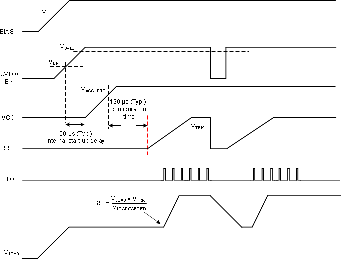
After the device configuration, a fast restart can be achieved without reconfiguration by toggling EN/UVLO when VH is greater than VSYNC. The device stops switching, but keeps the VCC regulator active when EN is less than VEN and VH is greater than VSYNC (See Figure 7-5).
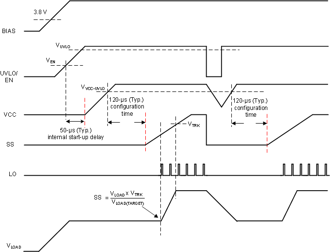
 Figure 7-4 Boost Start-up Waveforms Case
1: Start-up by EN/UVLO, Restart when VH < VSYNC
 Figure 7-5 Boost Start-up Waveforms Case
2: Start-up by EN/UVLO, Restart when VH > VSYNC