SLVSES8A October 2020 – December 2020 LM5127-Q1
PRODUCTION DATA
- 1 Features
- 2 Applications
- 3 Description
- 4 Revision History
- 5 Description (continued)
- 6 Pin Configuration and Functions
- 7 Specifications
-
8 Detailed Description
- 8.1 Overview
- 8.2 Functional Block Diagram
- 8.3
Feature Description
- 8.3.1 Device Enable (EN, VCC_HOLD)
- 8.3.2 Dual Input VCC Regulator (BIAS, VCCX, VCC)
- 8.3.3 Dual Input VDD Switch (VDD, VDDX)
- 8.3.4 Device Configuration and Light Load Switching Mode Selection (CFG/MODE)
- 8.3.5 Fixed or Adjustable Output Regulation Target (VOUT, FB)
- 8.3.6 Overvoltage Protection (VOUT, FB)
- 8.3.7 Power Good Indicator (PGOOD)
- 8.3.8 Programmable Switching Frequency (RT)
- 8.3.9 External Clock Synchronization (SYNC)
- 8.3.10 Programmable Spread Spectrum (DITHER)
- 8.3.11 Programmable Soft Start (SS)
- 8.3.12 Fast Re-start using VCC_HOLD (VCC_HOLD)
- 8.3.13 Transconductance Error Amplifier and PWM (COMP)
- 8.3.14 Current Sensing and Slope Compensation (CSA, CSB)
- 8.3.15 Constant Peak Current Limit (CSA, CSB)
- 8.3.16 Maximum Duty Cycle and Minimum Controllable On-time Limits (Boost)
- 8.3.17 Bypass Mode (Boost)
- 8.3.18 Minimum Controllable On-time and Minimum Controllable Off-time Limits (Buck)
- 8.3.19 Low Dropout Mode for Extended Minimum Input Voltage (Buck)
- 8.3.20 Programmable Hiccup Mode Overload Protection (RES)
- 8.3.21 MOSFET Drivers and Hiccup Mode Fault Protection (LO, HO, HB)
- 8.3.22 Battery Monitor (BMOUT, BMIN_FIX, BMIN_PRG)
- 8.3.23 Dual-phase Interleaved Configuration for High Current Supply (CFG)
- 8.3.24 Thermal Shutdown Protection
- 8.3.25 External VCCX Supply Reduces Power Dissipation
- 8.4 Device Functional Modes
- 9 Application and Implementation
- 10Power Supply Recommendations
- 11Layout
- 12Device and Documentation Support
- 13Mechanical, Packaging, and Orderable Information
パッケージ・オプション
メカニカル・データ(パッケージ|ピン)
- RGZ|48
サーマルパッド・メカニカル・データ
- RGZ|48
発注情報
9.3 System Examples
The BIAS and the SENSE1 pins should be connected to the output of the boost converter in this pre-boost + two single buck configuration.
 Figure 9-10 Pre-Boost + Two Single-phase Bucks Configuration
The BIAS and the SENSE1 pins should be connected to the output of the boost converter in this pre-boost + dual-phase buck configuration.
 Figure 9-11 Pre-Boost + Dual-phase Buck Configuration
The BIAS pin should be connected to the input of the buck converter in this three single buck configuration.
 Figure 9-12 Three Single-phase Bucks + Battery Monitor Configuration
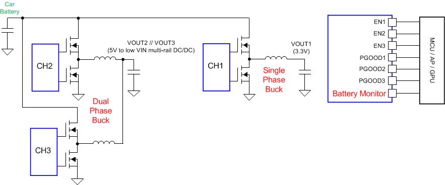
The BIAS pin should be connected to the input of the buck converter in this dual-phase buck + single buck configuration.
 Figure 9-13 Dual-phase Buck + Single-phase Buck + Battery Monitor Configuration
The BIAS and the SENSE1 pins should be connected to the output of the boost converter in this configuration.
 Figure 9-14 Two Single-phase Bucks in Parallel with Boost
Configuration
Figure 9-14 Two Single-phase Bucks in Parallel with Boost
ConfigurationThe BIAS and the SENSE1 pins should be connected to the buck converter input. The SW1 pins should be connected to the PGND1 pin. HO1 pin can be left floating. The HB1 pin should be connected to the VCC pin in non-synchronous boost configuration.
 Figure 9-15 Two Single-phase Bucks + Non-Synchronous Post-Boost Configuration
The BIAS pin should be connected to the buck converter input. The SENSE1 and SW1 pins should be connected to the PGND1 pin. HO1 should be connected to the high-side MOSFET through an AC coupling capacitor. HB1 should be connected to VCC in this synchronous SEPIC configuration.
 Figure 9-16 Dual-phase Buck in Parallel with Synchronous
SEPIC Configuration