JAJSCF1A August 2016 – November 2017 LM5161-Q1
PRODUCTION DATA.
- 1 特長
- 2 アプリケーション
- 3 概要
- 4 改訂履歴
- 5 Pin Configuration and Functions
- 6 Specifications
-
7 Detailed Description
- 7.1 Overview
- 7.2 Functional Block Diagram
- 7.3
Feature Description
- 7.3.1 Control Circuit
- 7.3.2 VCC Regulator
- 7.3.3 Regulation Comparator
- 7.3.4 Soft-Start
- 7.3.5 Error Transconductance (GM) Amplifier
- 7.3.6 On-Time Generator
- 7.3.7 Current Limit
- 7.3.8 N-Channel Buck Switch and Driver
- 7.3.9 Synchronous Rectifier
- 7.3.10 Enable / Undervoltage Lockout (EN/UVLO)
- 7.3.11 Thermal Protection
- 7.3.12 Ripple Configuration
- 7.4 Device Functional Modes
-
8 Applications and Implementation
- 8.1 Application Information
- 8.2
Typical Applications
- 8.2.1
LM5161-Q1 Synchronous Buck (15-V to 95-V Input, 12-V Output, 1-A Load)
- 8.2.1.1 Design Requirements
- 8.2.1.2
Detailed Design Procedure
- 8.2.1.2.1 Custom Design With WEBENCH® Tools
- 8.2.1.2.2 Output Resistor Divider Selection
- 8.2.1.2.3 Frequency Selection
- 8.2.1.2.4 Inductor Selection
- 8.2.1.2.5 Output Capacitor Selection
- 8.2.1.2.6 Series Ripple Resistor - RESR (FPWM = 1)
- 8.2.1.2.7 VCC and Bootstrap Capacitor
- 8.2.1.2.8 Input Capacitor Selection
- 8.2.1.2.9 Soft-Start Capacitor Selection
- 8.2.1.2.10 EN/UVLO Resistor Selection
- 8.2.1.3 Application Curves
- 8.2.2 LM5161-Q1 Isolated Fly-Buck (36-V to 72-V Input, 12-V, 12-W Isolated Output)
- 8.2.1
LM5161-Q1 Synchronous Buck (15-V to 95-V Input, 12-V Output, 1-A Load)
- 8.3 Do's and Don'ts
- 9 Power Supply Recommendations
- 10Layout
- 11デバイスおよびドキュメントのサポート
- 12メカニカル、パッケージ、および注文情報
パッケージ・オプション
メカニカル・データ(パッケージ|ピン)
- PWP|14
サーマルパッド・メカニカル・データ
- PWP|14
発注情報
7 Detailed Description
7.1 Overview
The LM5161-Q1 step-down switching regulator features all the functions needed to implement a low-cost, efficient buck converter capable of supplying 1-A to the load. This high voltage regulator contains 100-V N-channel buck and synchronous rectifier switches and is available in the 14-pin HTSSOP package. The regulator operation is based on constant ON-time control where the ON-time is inversely proportional to input voltage VIN. This feature maintains a relatively constant operating frequency with load and input voltage variations. A constant on-time switching regulator requires no loop compensation resulting in fast load transient response. Peak current limit detection circuit is implemented with a forced OFF-time during current limiting which is inversely proportional to voltage at the feedback pin, VFB and directly proportional to VIN. Varying the current limit OFF-time with VFB and VIN ensures short circuit protection with minimal current limit foldback. The LM5161-Q1 can be applied in numerous end equipment systems requiring efficient step-down regulation from higher input voltages. This regulator is well suited for 24 V industrial systems as well as for 48 V telecom and PoE voltage ranges. The LM5161-Q1 integrates an undervoltage lockout (EN/UVLO) circuit to prevent faulty operation of the device at low input voltages and features intelligent current limit and thermal shutdown to protect the device during overload or short circuit.
All instances of the LM5161 device name used throughout this document, in block diagrams and application schematics, are valid for LM5161-Q1 as well, unless stated otherwise.
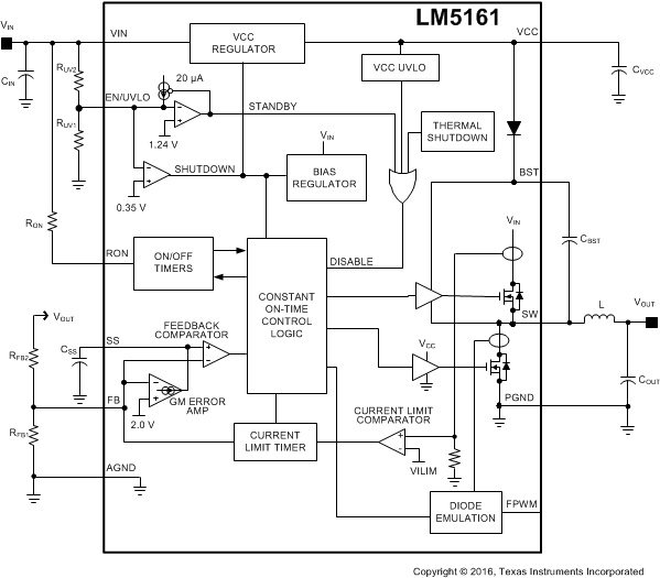
7.2 Functional Block Diagram

7.3 Feature Description
7.3.1 Control Circuit
The LM5161-Q1 step-down switching regulator employs a control principle based on a comparator and a one-shot ON-timer, with the output voltage feedback (FB) compared to the voltage at the Soft-Start (SS) pin (VSS). If the FB voltage is below VSS, the internal buck switch is turned on for a time period determined by the input voltage and one-shot programming resistor (RON). Following the ON-time, the buck switch must remain off for the minimum OFF-time forced by the minimum OFF-time one-shot. The buck switch remains off until the FB voltage falls below VSS again, when it turns on for another ON-time one-shot period.
During a rapid start-up or when the load current increases suddenly, the regulator operates with minimum off-time per cycle. When regulating the output in steady state operation, the off-time automatically adjusts to produce the SW pin duty cycle required for output voltage regulation.
When in regulation, the LM5161-Q1 operates in continuous conduction mode at heavy load currents. If the FPWM pin is connected to ground or left floating, the regulator operates in discontinuous conduction mode at light load with the synchronous rectifier FET emulating a diode. With sufficient load, the LM5161-Q1 operates in continuous conduction mode with the inductor current never reaching zero during the OFF-time of the high-side FET. In this mode the operating frequency remains relatively constant with load and line variations. The minimum load current for continuous conduction mode is one-half the inductor’s ripple current amplitude. The operating frequency (in Hz) is programmed by the RON pin resistor and can be calculated from Equation 1 with RON expressed in ohms.

In discontinuous conduction mode, current through the inductor ramps up from zero to a peak value during the ON-time, then ramps back to zero before the end of the OFF-time. The next ON-time period starts when the voltage at FB falls below VSS. When the inductor current is zero during the high side FET off-time, the load current is supplied by the output capacitor. In this mode, the operating switching frequency is lower than the continuous conduction mode switching frequency and the frequency varies with load. The discontinuous conduction mode maintains higher conversion efficiency at light loads since the switching losses decrease with the decrease in load and frequency.
The output voltage is set by two external resistors ( RFB1, RFB2). The regulated output voltage is calculated from Equation 2, where VREF = 2 V (typical) is the feedback reference voltage.

7.3.2 VCC Regulator
The LM5161-Q1 contains an internal high voltage linear regulator with a nominal output voltage of 7.3 V (typical). The VCC regulator is internally current limited to 30 mA (minimum). This regulator supplies power to internal circuit blocks including the synchronous FET gate driver and the logic circuits. When the voltage on the VCC pin reaches the undervoltage lockout (VCC(UV)) threshold of 3.98 V (typical), the IC is enabled. An external capacitor at the VCC pin stabilizes the regulator and supplies transient VCC current to the gate drivers. An internal diode connected from VCC to the BST pin replenishes the charge in the high-side gate drive bootstrap capacitor when the SW pin is low.
In high input voltage applications, the power dissipated in the regulator is significant and can limit the efficiency and maximum achievable output power. The LM5161-Q1 allows the internal VCC regulator power loss to be reduced by supplying the VCC voltage via a diode from an external voltage source regulated between 9 V and 13 V. The external VCC bias can be supplied from the LM5161-Q1 converter output rail if the regulation voltage is within this range. When the VCC pin of the LM5161-Q1 is raised above the regulation voltage (7.3 V typical), the internal regulator is disabled and the power dissipation in the IC is reduced.
7.3.3 Regulation Comparator
The feedback voltage at the FB pin is compared to the SS pin voltage VSS. In normal operation when the output voltage is in regulation, an ON-time period is initiated when the voltage at FB pin falls below VSS. The high-side buck switch stays on for the ON-time one-shot period causing the FB voltage to rise. After the on-time period expires, the high-side switch will remain off until the FB voltage falls below VSS. During start-up, the FB voltage is below VSS at the end of each on-time period and the high-side switch turns on again after the minimum forced off-time of 170 ns (typical). When the output is shorted to ground (FB = 0 V), the high side peak current limit is triggered, the high-side FET is turned off, and remains off for a period determined by the current limit OFF-time one-shot. See the Current Limit section for additional information.
7.3.4 Soft-Start
The soft-start feature of the LM5161-Q1 allows the converter to gradually reach a steady-state operating point, thereby reducing start-up stresses and current surges. When the EN/UVLO pin is above the EN/UVLO standby threshold VUVLO(TH) = 1.24 V (typical) and VCC exceeds the VCC undervoltage VCC(UV) = 3.98 V (typical) threshold, an internal 10-µA current source charges the external capacitor at the SS pin (CSS) from 0 V to 2 V. The voltage at the SS pin is connected to the noninverting input of the internal FB comparator. The soft-start interval ends when the SS capacitor is charged to the 2 V reference level. The ramping voltage at the SS pin produces a controlled, monotonic output voltage start-up. A minimum 1-nF soft-start capacitor must be used in all applications.
7.3.5 Error Transconductance (GM) Amplifier
The LM5161-Q1 provides a trans-conductance (GM) error amplifier that minimizes the difference between the reference voltage (VREF) and the average feedback (FB) voltage. This amplifier reduces the load and line regulation errors that are common in constant-on-time regulators. The soft-start capacitor (CSS) provides compensation for this error correction loop. The soft-start capacitor should be greater than 1 nF to ensure stability.
7.3.6 On-Time Generator
The ON-time of the LM5161-Q1 high-side FET is determined by the RON resistor and is inversely proportional to the input voltage (VIN). The inverse relationship with VIN results in a nearly constant frequency as VIN is varied. The ON-time can be calculated from Equation 3 with RON expressed in ohms.

To set a specific continuous conduction mode switching frequency (FSW expressed in Hz), the RON resistor is determined from Equation 4:

RON must be selected for a minimum on-time (at maximum VIN) greater than 150 ns for proper operation. This minimum ON-time requirement limits the maximum switching frequency of applications with relatively high VIN and low VOUT.
7.3.7 Current Limit
The LM5161-Q1 provides an intelligent current limit OFF-timer that adjusts the OFF-time to reduce foldback of the current limit. If the peak value of the current in the buck switch exceeds 1.6 A (typical) the present ON-time period is immediately terminated, and a non-resettable OFF-timer is initiated. The length of the OFF-time is controlled by the FB voltage and the input voltage VIN. As an example, when VFB = 0.1-V and VIN = 72-V, the OFF-time is set to 13 μs (typical). This condition would occur if the output is shorted or during the initial phase of start-up. In cases of output overload where the FB voltage is greater than zero volts (a soft short), the current limit OFF-time is reduced. Reducing the OFF-time during less severe overloads reduces the current limit foldback, overload recovery time, and start-up time. The current limit off-time, TOFF(CL) is calculated from Equation 5:

7.3.8 N-Channel Buck Switch and Driver
The LM5161-Q1 integrates an N-channel buck switch and associated floating high-side gate driver. The gate driver circuit works in conjunction with an external bootstrap capacitor and an internal high voltage bootstrap diode. A 10-nF or larger ceramic capacitor connected between the BST pin and the SW pin provides the voltage to the high-side driver during the buck switch ON-time. During the OFF-time, the SW node is pulled down to approximately 0 V and the bootstrap capacitor charges from VCC through the internal bootstrap diode. The minimum OFF-time of 170 ns (typical) provides a minimum time each cycle to recharge the bootstrap capacitor.
7.3.9 Synchronous Rectifier
The LM5161-Q1 provides an internal low-side synchronous rectifier N-channel FET. This low-side FET provides a low resistance path for the inductor current when the high-side FET is turned off.
With the FPWM pin connected to ground or left floating, the LM5161-Q1 synchronous rectifier operates in diode emulation mode. Diode emulation enables the pulse-skipping during light load conditions. This leads to a reduction in the average switching frequency at light loads. Switching losses and FET gate driver losses, both of which are proportional to switching frequency, are significantly reduced and efficiency is improved. This pulse-skipping mode also reduces the circulating inductor currents and losses associated with a continuous conduction mode (CCM). When the FPWM pin is grounded or left floating, an internal ripple injection circuit is enabled. With the internal ripple injection enabled, the typical external feedback ripple injection circuit is no longer required. This feature reduces the component count in the buck applications. For more details see Forced Pulse Width Modulation (FPWM) Mode.
When the FPWM pin is pulled high, diode emulation is disabled. The inductor current can flow in either direction through the low-side FET resulting in CCM operation with nearly constant switching frequency. A negative sink current limit circuit limits the current that can flow into the SW pin and through the low-side FET to ground. In a buck regulator application, large negative current will only flow from VOUT to the SW pin if VOUT is lifted above the output regulation set-point.
7.3.10 Enable / Undervoltage Lockout (EN/UVLO)
The LM5161-Q1 contains a dual level undervoltage lockout (EN/UVLO) circuit. When the EN/UVLO pin voltage is below 0.35 V (typical), the regulator is in a low current shutdown mode. When the EN/UVLO pin voltage is greater than 0.35 V (typical) but less than 1.24 V (typical), the regulator is in standby mode. In standby mode, the VCC bias regulator is active but converter switching remains disabled. When the voltage at the VCC pin exceeds the VCC rising threshold VCC(UV) = 3.98 V (typical) and the EN/UVLO pin voltage is greater than 1.24 V, normal switching operation begins. An external resistor voltage divider from VIN to GND can be used to set the minimum operating voltage of the regulator.
EN/UVLO hysteresis is accomplished with an internal 20-μA (typical) current source (IUVLO(HYS)) that is switched on or off into the impedance of the EN/UVLO pin resistor divider. When the EN/UVLO threshold is exceeded, the current source is activated to effectively raise the voltage at the EN/UVLO pin. The hysteresis is equal to the value of this current times the upper resistance of the resistor divider, (RUV2) (See Functional Block Diagram).
7.3.11 Thermal Protection
The LM5161-Q1 must be operated such that the junction temperature does not exceed 150°C during normal operation. An internal thermal shutdown circuit is provided to protect the LM5161-Q1 in the event of a higher than normal junction temperature. When activated, typically at 175°C, the controller is forced into a low-power reset state, disabling the high side buck switch and the VCC regulator. This feature prevents catastrophic failures due to device overheating. When the junction temperature falls below 155°C (typical hysteresis = 20°C), the VCC regulator is enabled, and operation resumes.
7.3.12 Ripple Configuration
LM5161-Q1 uses a Constant-On-Time (COT) control scheme, in which the ON-time is terminated by a one-shot, and the OFF-time is terminated by the feedback voltage (VFB) falling below the reference voltage. Therefore, for stable operation, the feedback voltage must decrease monotonically and in phase with the inductor current during the OFF-time. Furthermore, this change in feedback voltage (VFB) during OFF-time must be large enough to dominate any noise present at the feedback node.
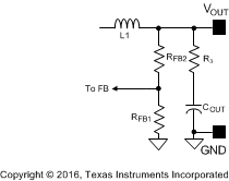
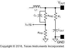
Table 1 presents three different methods for generating appropriate voltage ripple at the feedback node. Type 1 and Type 2 ripple circuits couple the ripple from the output of the converter to the feedback node (FB). The output voltage ripple has two components:
- Capacitive ripple caused by the inductor current ripple charging or discharging the output capacitor.
- Resistive ripple caused by the inductor current ripple flowing through the ESR of the output capacitor and R3.
The capacitive ripple is out-of-phase with the inductor current. As a result, the capacitive ripple does not decrease monotonically during the OFF-time. The resistive ripple is in phase with the inductor current and decreases monotonically during the OFF-time. The resistive ripple must exceed the capacitive ripple at output (VOUT) for stable operation. If this condition is not satisfied unstable switching behavior is observed in COT converters, with multiple ON-time bursts in close succession followed by a long OFF-time.
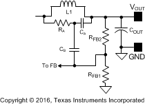
Type 3 ripple method uses a ripple injection circuit with RA, CA and the switch node (SW) voltage to generate a triangular ramp. This triangular ramp is then AC-coupled into the feedback node (FB) using the capacitor CB. Since this circuit does not use the output voltage ripple, it is suited for applications where low output voltage ripple is imperative. See application note Controlling Output Ripple and Achieving ESR Independence in Constant On-Time (COT) Regulator Designs (SNVA166) for more details for each ripple generation method.
Table 1. Ripple Configuration
| TYPE 1 | TYPE 2 | TYPE 3 |
|---|---|---|
| Lowest Cost | Reduced Ripple | Minimum Ripple |
 |
 |
 |
|
Equation 6.
 |
Equation 7.
 |
Equation 8.
 |
7.4 Device Functional Modes
7.4.1 Forced Pulse Width Modulation (FPWM) Mode
The Synchronous Rectifier section gives a brief introduction to the LM5161-Q1 diode emulation feature. The FPWM pin allows the power supply designer to select either CCM or DCM mode of operation at light loads. When the FPWM pin is connected to ground or left floating (FPWM = 0), a pulse-skipping mode and the zero-cross current detector circuit is enabled. The zero-cross detector turns off the low-side FET when the inductor current falls close to zero (IZX, see Electrical Characteristics). This feature allows the LM5161-Q1 regulator to operate in DCM mode at light loads. In the DCM state, the switching frequency decreases with lighter loads.
When the FPWM pin is left open or shorted to ground, the user can take the advantage of the internal ripple injection circuit, enabled in this mode, for a typical Buck application circuit. This feature is applicable over the entire load and input voltage ranges. It eliminates the need for an external feedback ripple injection circuit.
For wide VIN applications where VIN > 72 V, an external VCC supply is commonly used to minimize the power dissipation in the IC. In such applications at TJ >125°C, it is recommended to add a BST resistor (> 3Ω) in series with the BST capacitor, in order to protect the internal VCC-BST diode during a full load transient operation. The addition of the external resistor will reduce the fast (dv/dt) of the switch node that can impact the normal IC operation.
If the FPWM pin is pulled high, the LM5161-Q1 will operate in CCM mode regardless of the load conditions. The CCM operation reduces efficiency at light load but improves the output transient response to step load changes and provides nearly constant switching frequency. Moreover, the Fly-Buck topology always requires the continuous conduction mode during its operation.
The internal ripple injection circuit is disabled in the CCM mode. An external ripple injection circuit or an additional ESR resistor in series with the output capacitor is required to generate the optimal ripple at the FB node. Also, there is no need to add any BST resistor in series with the BST capacitor in either forced CCM Buck or Fly-Buck application.
Table 2. FPWM Pin Mode Summary
| FPWM PIN CONNECTION | LOGIC STAGE | DESCRIPTION |
|---|---|---|
| GND or Floating (High Z) | 0 | The FPWM pin is grounded or left floating. DCM enabled at light loads. Internal Ripple circuit is enabled. No external ripple circuit/ addition required. |
| VCC | 1 | The FPWM pin is connected to VCC. The LM5161-Q1 then operates in CCM mode at light loads. Internal ripple injection disabled. External ripple injection needed. |
7.4.2 Undervoltage Detector
The following table summarizes the dual threshold levels of the undervoltage lockout (EN/UVLO) circuit explained in Enable / Undervoltage Lockout (EN/UVLO).
Table 3. UVLO Pin Mode Summary
| EN/UVLO PIN VOLTAGE | VCC REGULATOR | MODE | DESCRIPTION |
|---|---|---|---|
| < 0.35 V | Off | Shutdown | VCC regulator disabled. High and low side FETs disabled. |
| 0.35 V to 1.24 V | On | Standby | VCC regulator enabled. High and low side FETs disabled. |
| > 1.24 V | VCC < VCC(UV) | Standby | VCC regulator enabled. High and low side FETs disabled. |
| VCC > VCC(UV) | Operating | VCC regulator enabled. Switching enabled. |
If an EN/UVLO setpoint is not required, the EN/UVLO pin can be driven by a logic signal as an enable input or connected directly to the VIN pin. If the EN/UVLO is directly connected to the VIN pin, the regulator will begin switching when the VCC UVLO is satisfied.