JAJSKQ3D February 2016 – December 2022 LM5165
PRODUCTION DATA
- 1 特長
- 2 アプリケーション
- 3 概要
- 4 Revision History
- 5 Pin Configuration and Functions
- 6 Specifications
-
7 Detailed Description
- 7.1 Overview
- 7.2 Functional Block Diagram
- 7.3
Feature Description
- 7.3.1 Integrated Power MOSFETs
- 7.3.2 Selectable PFM or COT Mode Converter Operation
- 7.3.3 COT Mode Light-Load Operation
- 7.3.4 Low Dropout Operation and 100% Duty Cycle Mode
- 7.3.5 Adjustable Output Voltage (FB)
- 7.3.6 Adjustable Current Limit
- 7.3.7 Precision Enable (EN) and Hysteresis (HYS)
- 7.3.8 Power Good (PGOOD)
- 7.3.9 Configurable Soft Start (SS)
- 7.3.10 Thermal Shutdown
- 7.4 Device Functional Modes
-
8 Applications and Implementation
- 8.1 Application Information
- 8.2
Typical Applications
- 8.2.1 Design 1: Wide VIN, Low IQ COT Converter Rated at 5 V, 150 mA
- 8.2.2 Design 2: Small Solution Size PFM Converter Rated at 3.3 V, 50 mA
- 8.2.3 Design 3: High Density 12-V, 75-mA PFM Converter
- 8.2.4 Design 4: 3.3-V, 150-mA COT Converter With High Efficiency
- 8.2.5 Design 5: 15-V, 150-mA, 600-kHz COT Converter
- 8.3 Power Supply Recommendations
- 8.4 Layout
- 9 Device and Documentation Support
- 10Mechanical, Packaging, and Orderable Information
パッケージ・オプション
メカニカル・データ(パッケージ|ピン)
- DRC|10
サーマルパッド・メカニカル・データ
- DRC|10
発注情報
5 Pin Configuration and Functions
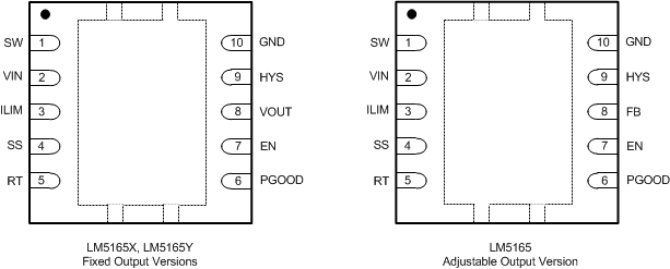
 Figure 5-1 DRC Package10-Pin VSON With Exposed
Thermal Pad(Top View)
Figure 5-1 DRC Package10-Pin VSON With Exposed
Thermal Pad(Top View)Table 5-1 Pin Functions
| PIN | TYPE(1) | DESCRIPTION | |
|---|---|---|---|
| NO. | NAME | ||
| 1 | SW | P | Switching node that is internally connected to the drain of the high-side PMOS buck switch and the drain of the low-side NMOS synchronous rectifier. Connect to the switching side of the power inductor. |
| 2 | VIN | P | Regulator supply input pin to high-side power MOSFET and internal bias rail LDO. Connect to input supply and input capacitor CIN. Path from VIN to the input capacitor must be as short as possible. |
| 3 | ILIM | I | Programming pin for current limit. Connecting the appropriate resistor from ILIM to GND selects one of four preset current limit options. Short ILIM to GND for the maximum current setting. |
| 4 | SS | I | Programming pin for the soft-start time. If a 100-kΩ resistor is connected from SS to GND, the internal soft-start circuit is disabled and the FB comparator reference steps immediately from zero to full value when the regulator is enabled by the EN input. If the SS pin is left open, the internal soft-start circuit ramps the FB reference from zero to full value in 900 µs. If an appropriate capacitance is connected to the SS pin, the soft-start time can be programmed as required. |
| 5 | RT | I | Mode selection and on-time programming pin for Constant On-Time (COT) control. Short RT to GND to select PFM (pulse frequency modulation) operation. Connect a resistor from RT to GND to program the on-time, which sets the switching frequency for COT. |
| 6 | PGOOD | O | Power Good output flag pin. PGOOD is connected to the drain of an NFET that holds the pin low when either FB or VOUT is below the regulation target. Use a pullup resistor of 10 kΩ to 100 kΩ to the system voltage rail or VOUT (no higher than 12 V). |
| 7 | EN | I | Input pin of the precision enable / UVLO comparator. The converter is enabled when the EN voltage is greater than 1.212 V. |
| 8 | VOUT/FB | I | Feedback input to voltage regulation loop. The VOUT pin connects the internal feedback resistor divider to the regulator output voltage for fixed 3.3-V and 5-V options. The FB pin connects the internal feedback comparator to an external resistor divider for the adjustable output voltage option. The FB comparator reference voltage is nominally 1.223 V. |
| 9 | HYS | O | Drain of an internal NFET that is turned off when the EN input is greater than the EN threshold. An external resistor from HYS to the EN pin UVLO resistor divider programs the input UVLO hysteresis voltage. |
| 10 | GND | G | Regulator ground return |
| — | PAD | P | Exposed pad. Connect to the GND pin and system ground on PCB. Path to CIN must be as short as possible. |
(1) P = Power, G = Ground, I = Input, O = Output.