JAJSNH1A December 2021 – September 2022 LM5168 , LM5169
PRODUCTION DATA
- 1 特長
- 2 アプリケーション
- 3 概要
- 4 Revision History
- 5 Device Comparison Table
- 6 Pin Configuration and Functions
- 7 Specifications
-
8 Detailed Description
- 8.1 Overview
- 8.2 Functional Block Diagram
- 8.3
Feature Description
- 8.3.1 Control Architecture
- 8.3.2 Internal VCC Regulator and Bootstrap Capacitor
- 8.3.3 Internal Soft Start
- 8.3.4 On-Time Generator
- 8.3.5 Current Limit
- 8.3.6 N-Channel Buck Switch and Driver
- 8.3.7 Synchronous Rectifier
- 8.3.8 Enable, Undervoltage Lockout (EN/UVLO)
- 8.3.9 Power Good (PGOOD)
- 8.3.10 Thermal Protection
- 8.4 Device Functional Modes
-
9 Application and Implementation
- 9.1 Application Information
- 9.2
Typical Fly-Buck™ Converter Application
- 9.2.1 Design Requirements
- 9.2.2
Detailed Design Procedure
- 9.2.2.1 Switching Frequency (RT)
- 9.2.2.2 Transformer Selection
- 9.2.2.3 Output Capacitor Selection
- 9.2.2.4 Secondary Output Diode
- 9.2.2.5 Setting Output Voltage
- 9.2.2.6 Input Capacitor
- 9.2.2.7 Type-3 Ripple Network
- 9.2.2.8 CBST Selection
- 9.2.2.9 Minimum Secondary Output Load
- 9.2.2.10 Example Design Summary
- 9.2.3 Application Curves
- 9.3 Typical Buck Application
- 9.4 Power Supply Recommendations
- 9.5 Layout
- 10Device and Documentation Support
- 11Mechanical, Packaging, and Orderable Information
パッケージ・オプション
メカニカル・データ(パッケージ|ピン)
- DDA|8
サーマルパッド・メカニカル・データ
- DDA|8
発注情報
8.3.5 Current Limit
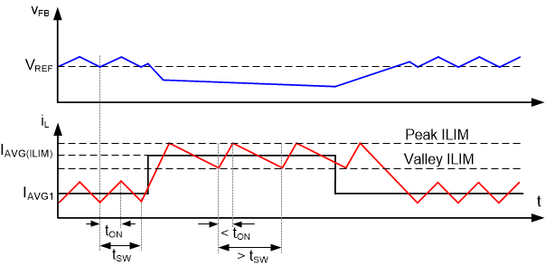
The LM5168P manages overcurrent conditions with cycle-by-cycle current limiting of the peak inductor current. The current sensed in the high-side MOSFET is compared every switching cycle to the current limit threshold (0.42 A typical). To protect the converter from potential current runaway conditions, the LM5168P includes a fold-back valley current limit feature, set at 0.34 A, that is enabled if a peak current limit is detected. As shown in Figure 8-1, if the peak current in the high-side MOSFET exceeds 0.42 A for the LM5168P (typical), the present cycle is immediately terminated regardless of the programmed on time (tON), the high-side MOSFET is turned off and the fold-back valley current limit is activated. The low-side MOSFET remains on until the inductor current drops below this fold-back valley current limit, after which the next on-pulse is initiated. This method folds back the switching frequency to prevent overheating and limits the average output current to less than 0.3 A for LM5168P to ensure proper short-circuit and heavy-load protection.
 Figure 8-1 Current Limit Timing Diagram
Current is sensed after a leading-edge blanking time following the high-side MOSFET turn-on transition. The propagation delay of the current limit comparator is 100 ns. During high step-down conditions when the on time is less than 100 ns, a backup peak current limit comparator in the low-side FET also set at 0.84 A or 0.42 A, enables the foldback valley current limit set at 0.67 A or 0.34 A. This innovative current limit scheme enables ultra-low duty-cycle operation, permitting large step-down voltage conversions while ensuring robust protection of the converter.
The LM5168F, LM5169F, and LM5169P implement a current limit off-timer and hiccup protection. If the current in the high-side MOSFET exceeds IHS_PK(OC), the high-side MOSFET is immediately turned off and a non-resettable off-timer is initiated. The length of the off time is controlled by the feedback voltage and the input voltage. The off-timer ensures safe short circuit operation in a fly-buck converter configuration. An overload current on the secondary output can result in the secondary voltage collapsing while the primary voltage remains in regulation. This action results in a possible condition where the secondary output voltage does not recover after the overload condition. Hiccup protection makes sure a soft-start counter enables both the secondary and primary output voltages to recover properly after an overcurrent event is detected for 16 consecutive current limit cycles. After four consecutive cycles without current limit detection, restart the hiccup protection counter. These devices attempt soft start after a "hiccup period" of 64 ms.